Fix iPhone 11 Pro Max Won't Turn On
Prior to commencing any repair work, disconnect the device entirely from all electrical power connections to guarantee safety.
- The following implements are necessary to complete the repair procedure:A Phillips head screwdriver is needed for disassembly and reassembly.
Should difficulties arise while performing the repair, refer to the device's official documentation or contact a qualified technician for support.
Step 1 | Fix iPhone 11 Pro Max Won't Turn On


- The device fails to initiate its operating system.
- Carefully separate the display assembly from the chassis, then detach the battery connector, and subsequently apply power to the motherboard via a test lead.A current measurement of 1 Ampere is observed during this procedure.An abnormally high current draw, even without successful system startup, indicates a problem within the primary power management circuitry and its associated components.
Step 2


- Proceed with detaching the motherboard from the device.
- Utilize a multimeter to determine the diode value present at the battery connector, which should register as 314, indicating proper function.Employing a thermal imager, position the motherboard to observe its temperature distribution; connect it to a power source for this assessment.Significant heat is detected in regions surrounding the NAND flash memory components.
- Because the NAND memory is not directly powered by the main circuit, isolating the motherboard is necessary for more detailed diagnostics.
Step 3


- Detach the logic board, which incorporates the heating platform, from the device.The heating platform operates at a temperature of 170 degrees Celsius.Prior physical trauma to the device is evident through the observation of numerous missing bonding pads.
- These absent bonding pads indicate significant damage resulting from the observed drop impact.
Step 4


- Following this, establish an electrical connection between the logic board and a power source, noting that the logic board's current draw is minimal, suggesting the issue likely resides within the signal board.
- Isolate the signal board and apply power using multimeter probes to observe its current consumption; a significant current reading confirms the fault's location on the signal board.
Step 5


- Employing a thermal imaging device to identify the source of the problem necessitates powering the signal board while it is positioned under the imager.The area surrounding the component designated as "U5000" exhibits a rapid temperature increase, typically reaching 80 degrees Celsius.Utilize a multimeter to assess the capacitance values of the components situated near "U5000"; a short circuit condition is present.
- During the capacitance measurement process, a visually damaged, burnt-out capacitor was also discovered.The identification of the fault requires the use of a thermal imager, which should be powered during the diagnostic procedure.A short circuit condition is indicated by multimeter readings taken on the capacitors located in the vicinity of "U5000".
Step 6


- Following this, the capacitor must be detached from the circuit board.To facilitate soldering, apply a thin layer of Paste Flux to the capacitor's leads.Utilize a Hot Air Gun, set to a temperature of 380 degrees Celsius, to carefully desolder and remove the component.
- A replacement capacitor should then be installed in the vacated position.
- Verify the diode's functionality once more using a multimeter; a healthy reading should indicate a value of 446.
Step 7


- To address the remaining pad deficiencies, these areas necessitate repair procedures.Employ a Soldering Iron to eliminate excess solder from the signal board's bonding pads.Utilize Solder Wick in conjunction with the Soldering Iron to achieve thorough tin removal from the bonding pads.Apply the identical cleaning process to the logic board's bonding pads, subsequently removing the thermal paste residue.Continue the cleaning process of the bonding pads using PCB Cleaner to ensure a pristine surface.
- Consult the REFOX Bitmap software to precisely identify the locations of missing pads requiring repair.
Step 8


- If certain absent pads lack a connection to ground, repair efforts are unnecessary.Utilize a 'Sculpture Knife' to expose the underlying circuit traces for any remaining missing pads.Employ a 'Soldering Iron' to apply solder to the bonding pads, ensuring proper contact.
- Position the 'Soldering Lugs' precisely onto the bonding pads.Secure the 'Soldering Lugs' using a 'Soldering Iron' heated to 380 degrees Celsius.Following the soldering process, apply 'Solder Mask' to the newly repaired bonding pads.Expose the repaired bonding pads to a UV Lamp for a duration of 5 minutes to facilitate hardening.The absence of a ground connection renders pad repair superfluous in specific instances.Exposing the circuit traces beneath the missing pads requires the careful use of a 'Sculpture Knife'.Solder deposition onto the bonding pads is achieved through the application of heat from a 'Soldering Iron'.
- Accurate placement of the 'Soldering Lugs' is crucial for a reliable connection.A temperature of 380 °C is recommended when using a 'Soldering Iron' to secure the 'Soldering Lugs'.UV lamp exposure for 5 minutes is essential for the proper curing of the applied 'Solder Mask'.
Step 9


- Once the solder mask has completely hardened, utilize a "Sculpture Knife" to eliminate any surplus material, thereby exposing the necessary pads.The subsequent step involves reballing the signal board, beginning with the uniform distribution of a thin layer of low-temperature solder paste across its surface.To facilitate the reballing process, position the signal board onto a heating platform maintained at a temperature of 170 °C.
- Heat application is essential for proper solder flow and component adhesion during the reballing procedure.
- Employing a "Sculpture Knife" allows for precise removal of excess solder mask, revealing the underlying pads for subsequent operations.
Step 10


- Following the creation of solder ball connections and subsequent cooling of the printed circuit board, a bonding pad flux application is necessary.
- Ensure precise positioning of the circuit board.
Step 11
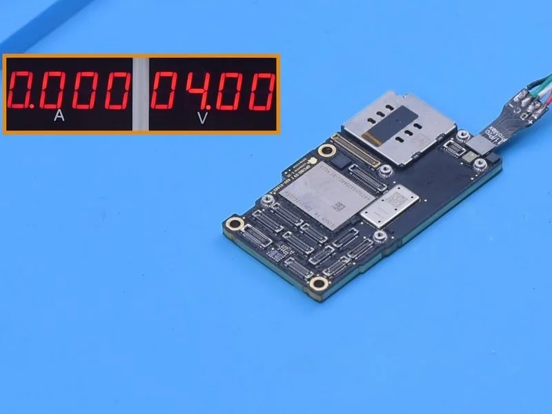


- Following the reassembly process and allowing the motherboard to return to ambient temperature, establish a connection utilizing a Power Cable.The absence of a substantial electrical flow across the motherboard is now confirmed.Initiate the power-on sequence by employing Tweezers, which restores the typical boot current levels.
Secure the motherboard within the device's chassis to complete the reinstallation.
Successful device activation is indicated, alongside the expected functionality of the baseband system.