Apple A6 Teardown
Chipworks has provided an in-depth analysis of Apple’s A6 Processor, and this collaboration allows us to explore its design, including the anticipated two custom CPUs operating at a clock speed of 1 GHz and utilizing the ARMv7s instruction set. The teardown will also showcase the specialized equipment and instruments employed by Chipworks.
- Stay informed about iFixit's latest news, guides, and product teardowns by following us on Twitter at @iFixit or visiting our page on The Book.
Step 1 | Apple A6 Teardown

Begin the procedure.For this iteration of Science with iFixit, Chipworks provided expert assistance.
Before proceeding, please be aware that this procedure involves potential hazards and requires careful attention to detail; failure to adhere to safety precautions could result in injury or equipment damage.Expect to encounter specialized terminology throughout this disassembly process; explanations will be provided where possible, but supplemental information may be found via Wikipedia references.
Let’s explore the features that make the A6 model popular.
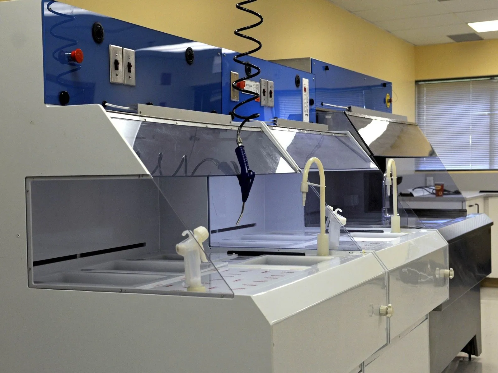
Before proceeding, understand the specialized Chipworks machinery crucial for these procedures.
Before proceeding, please be aware that this procedure involves potential hazards and requires careful attention to detail; failure to adhere to safety precautions could result in injury or equipment damage.Expect to encounter specialized terminology throughout this disassembly process; explanations will be provided where possible, but supplemental information may be found via Wikipedia references.
Let’s explore the features that make the A6 model popular.
Before proceeding, understand the specialized Chipworks machinery crucial for these procedures.
Step 2 | Life at Chipworks
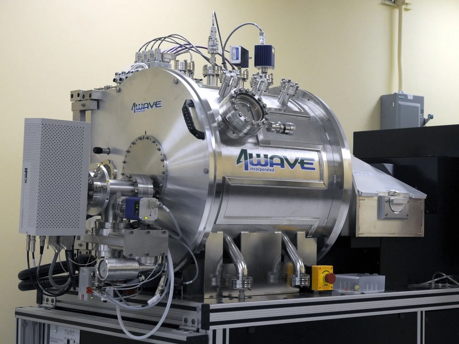
Employ specialized microelectronics fabrication techniques.The device incorporates a genuine ion blaster, informally known as Ibe, with a maximum output of 3.2 gigawatts and a recharge time of 17 seconds.Employing a focused beam of ions to selectively remove material from a substrate.).
Semiconductor device material is precisely and selectively etched away in thin, flat layers using an Ibe process.
Employing a process analogous to sandblasting, ion beam etching selectively removes material from a semiconductor wafer; however, instead of abrasive particles, a focused beam of ionized atoms serves as the etchant.
The Apple A6 chip, manufactured using Samsung's 32 nm HKMG (high-k dielectric, metal gate) CMOS fabrication process, exemplifies modern semiconductor construction utilizing varied materials, a characteristic that highlights the importance of specialized diagnostic equipment.
This device functions as an ion-based energy weapon.
Step 3
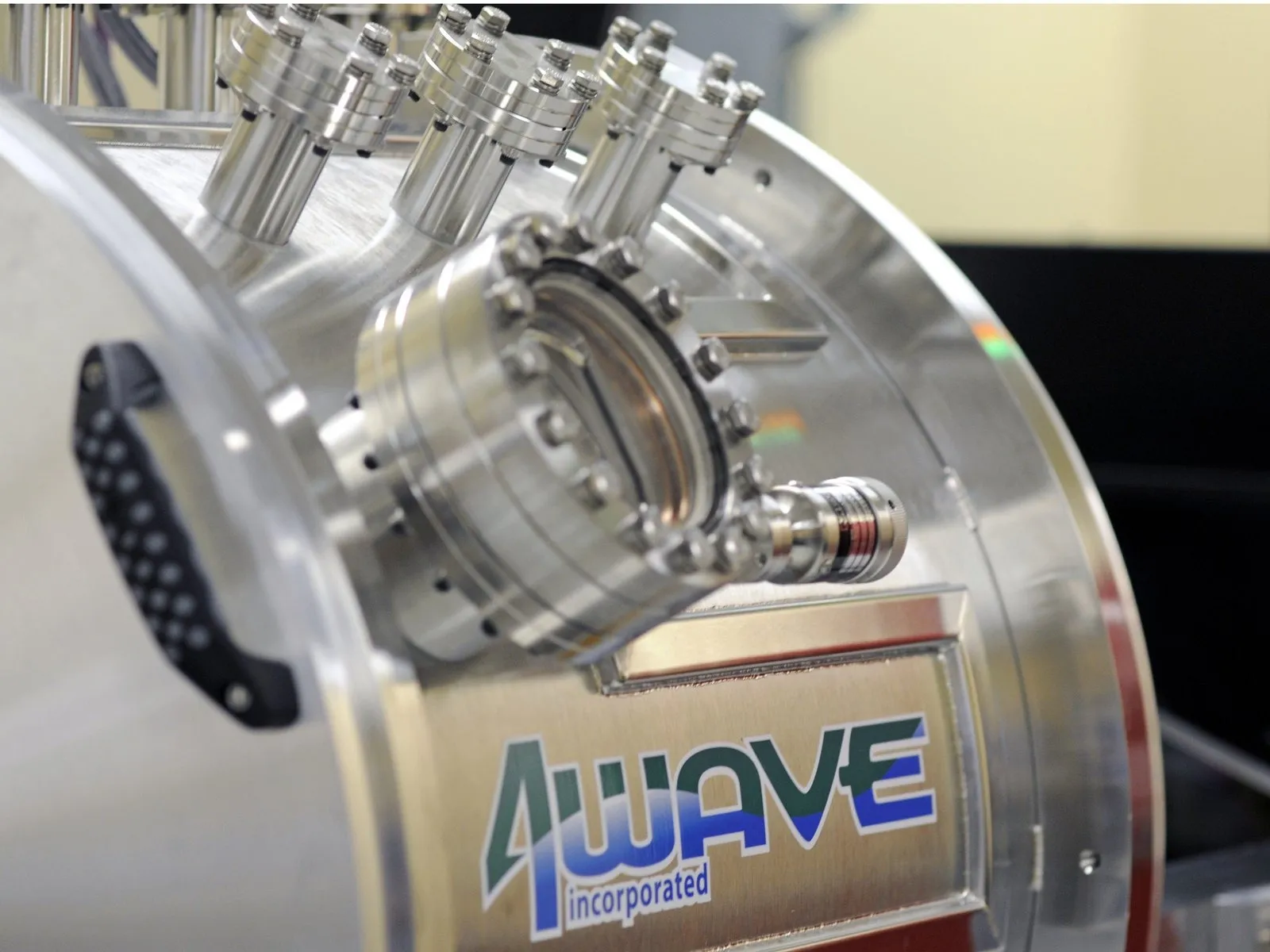
A developer from Chipworks was involved.Configure the Ibe system to facilitate dielectric material removal from advanced node chips, such as the A6, which can incorporate up to nine copper layers, one aluminum layer, along with polysilicon and substrate layers.
Chipworks has expanded its de-layering laboratory with supplementary wet benches, fume hoods, and polishing stations.
Chipworks has expanded its de-layering laboratory with supplementary wet benches, fume hoods, and polishing stations.
Step 4
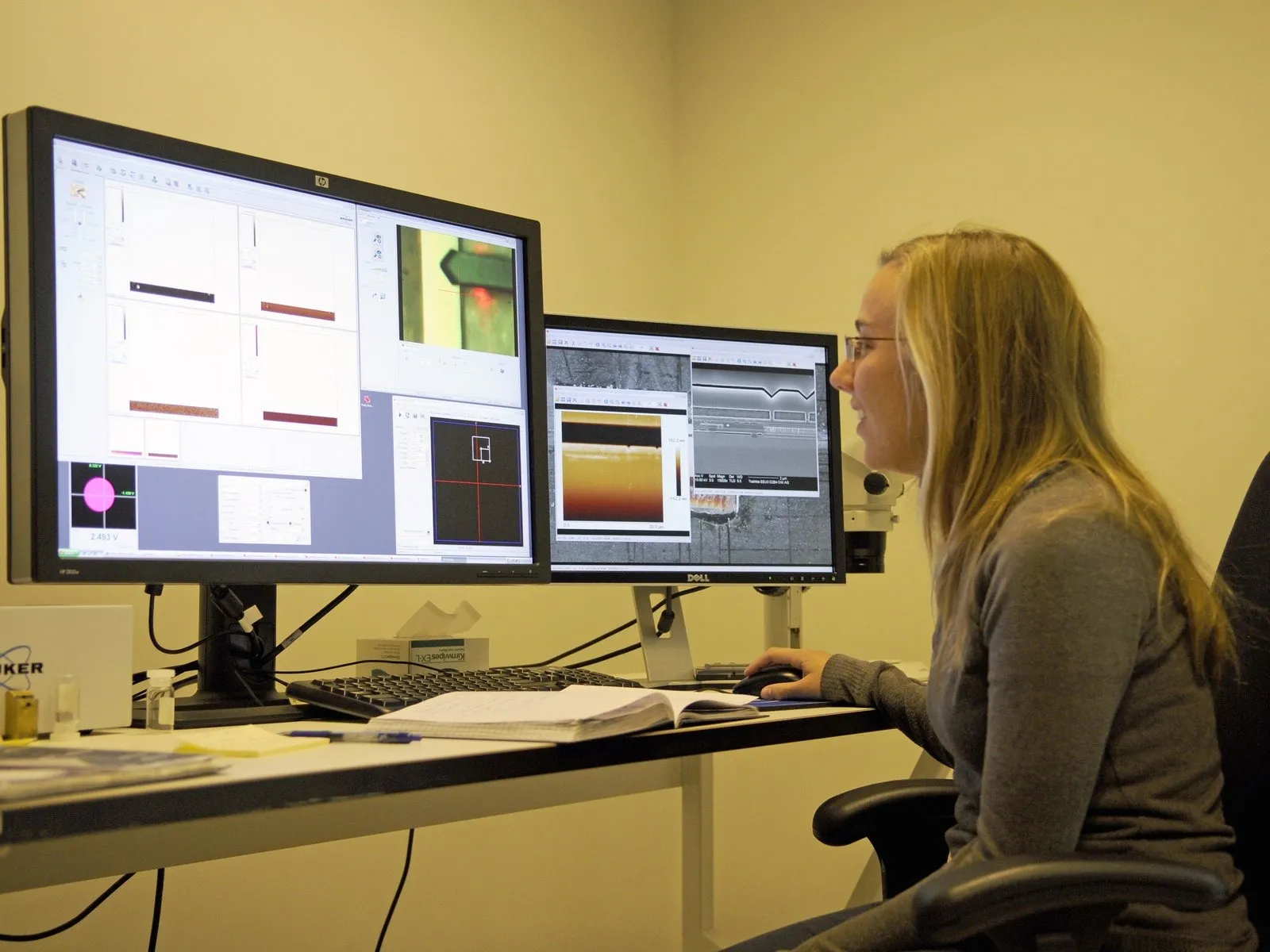

The concentration and distribution of impurities introduced into the semiconductor material must be precisely controlled.A thorough grasp of these principles is essential for comprehending the operational mechanisms and internal design of modern, sophisticated electronics.
The A6's NMOS and PMOS device doping profiles, and the doping methods used for the 8-megapixel iSight camera's photo cathodes, are now analyzable thanks to Chipworks' acquisition of a scanning capacitance microscope featuring enhanced resolution.
The A6's NMOS and PMOS device doping profiles, and the doping methods used for the 8-megapixel iSight camera's photo cathodes, are now analyzable thanks to Chipworks' acquisition of a scanning capacitance microscope featuring enhanced resolution.
Step 5


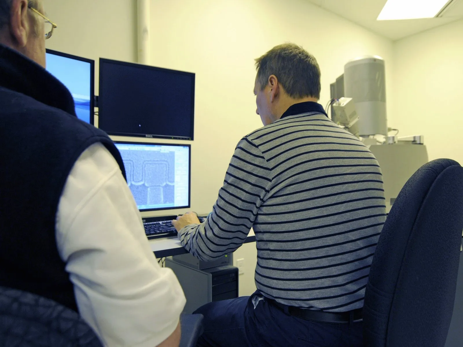
Employ scientific principles and methodologies.
Following A6 preparation, process and development technicians analyze the outcomes, utilizing optical microscopes to observe intermediate stages and adjust processing parameters for optimal results.
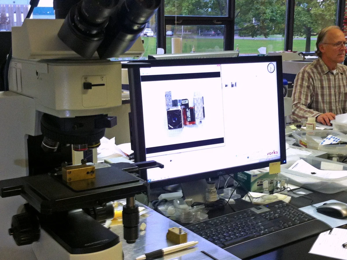
To identify the camera's manufacturer, a detailed microscopic examination of the rear-facing iSight camera's internal components is necessary, as this information is not readily accessible.
Chipworks’ expertise rapidly resolved the complex analysis required to understand the device's internal construction.
Following A6 preparation, process and development technicians analyze the outcomes, utilizing optical microscopes to observe intermediate stages and adjust processing parameters for optimal results.
To identify the camera's manufacturer, a detailed microscopic examination of the rear-facing iSight camera's internal components is necessary, as this information is not readily accessible.
Chipworks’ expertise rapidly resolved the complex analysis required to understand the device's internal construction.
Step 6
To examine transistor strain, gate oxide thicknesses, or crystal lattice orientation, utilize the scanning electron microscope.
The transmission electron microscope’s high-resolution imaging capability stems from utilizing electrons, whose de Broglie wavelength is notably small—a direct consequence of quantum mechanical principles.
Transmission electron microscopy functions by directing a focused beam of electrons toward a sample, and subsequently analyzing the resulting interactions to reveal material properties.
Chipworks utilizes specialized equipment and methods to generate the detailed visuals presented on their website, though certain proprietary processes remain undisclosed; consequently, we will now examine the internal components of iPhone 5 chips.
Step 7 | Inside the iPhone 5
According to Chipworks, this model features numerous innovative parts and is considered Apple's strongest release since the original iPhone.
The following components will be examined.
The following components will be examined.
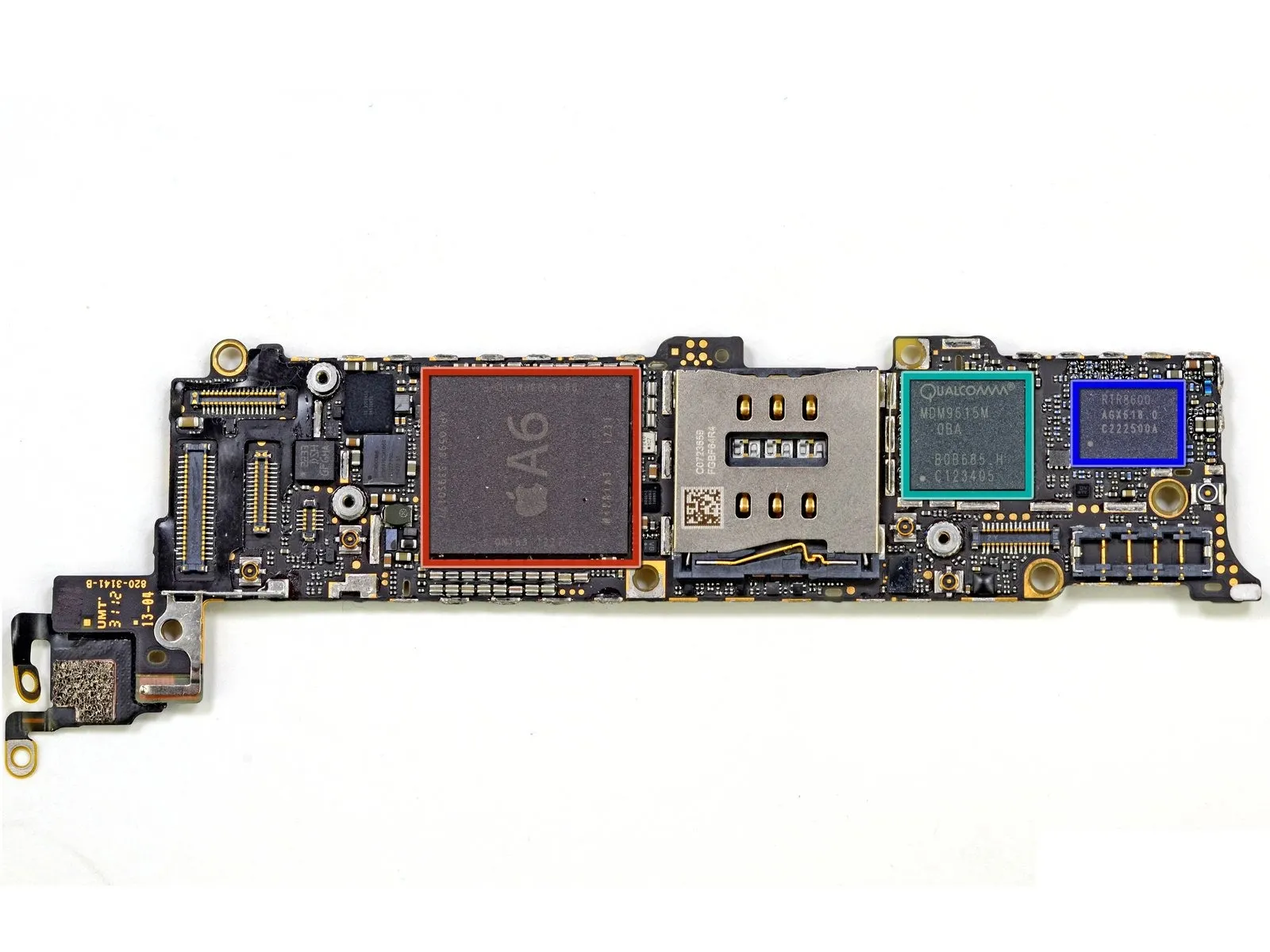
- The device utilizes an Apple A6 application processor.
- The audio processing component is designated as a Cirrus chip, model number 338S1077, by Apple.
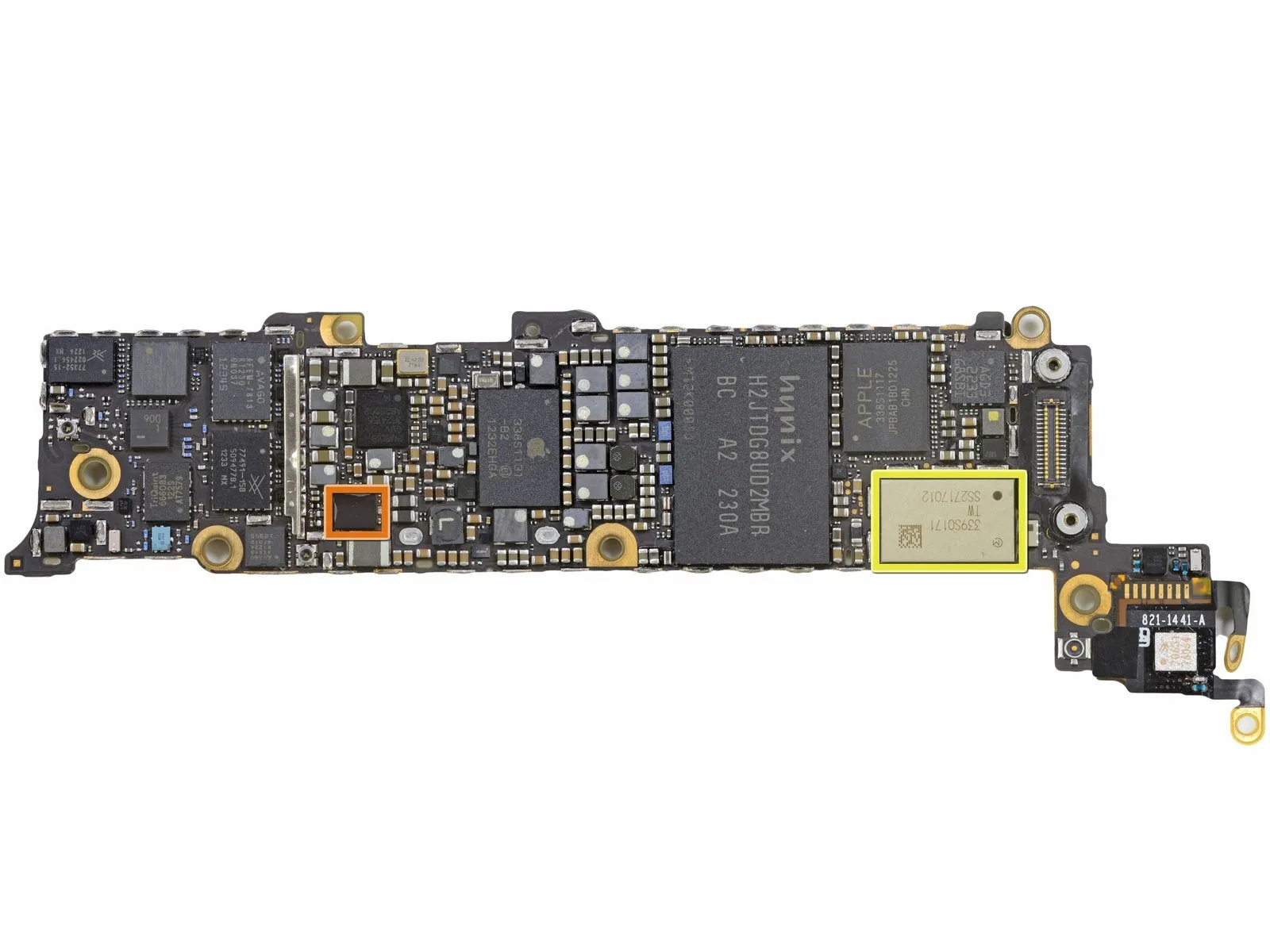
- Wi-Fi functionality is provided by the Murata 339S0171 module.
- LTE modem: Qualcomm MDM9615
- The device is a Qualcomm RTR8600, functioning as a radio frequency transceiver supporting multiple bands and operational modes.
Step 8 | The A6 Processor
To investigate the A6's internal components, begin by creating an access point through its housing.
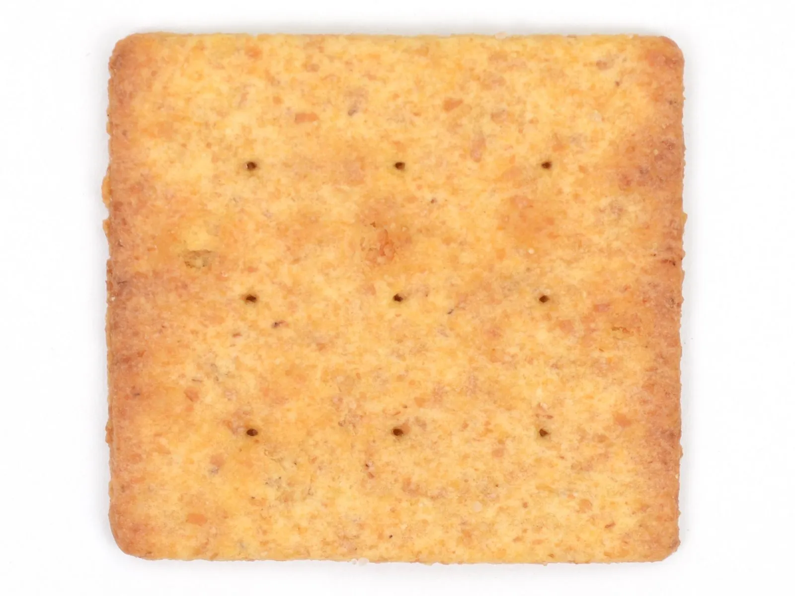
The exposed surface of an A6 processor's metal die closely resembles the shape and appearance of a Wheat Thin cracker.
Chipworks employed a detailed process, beginning with photographing a single Wheat Thin.
To remove the A6 component's protective casing, immerse it in a heated solution of fuming sulfuric acid, maintaining a temperature optimized for effective decapsulation.
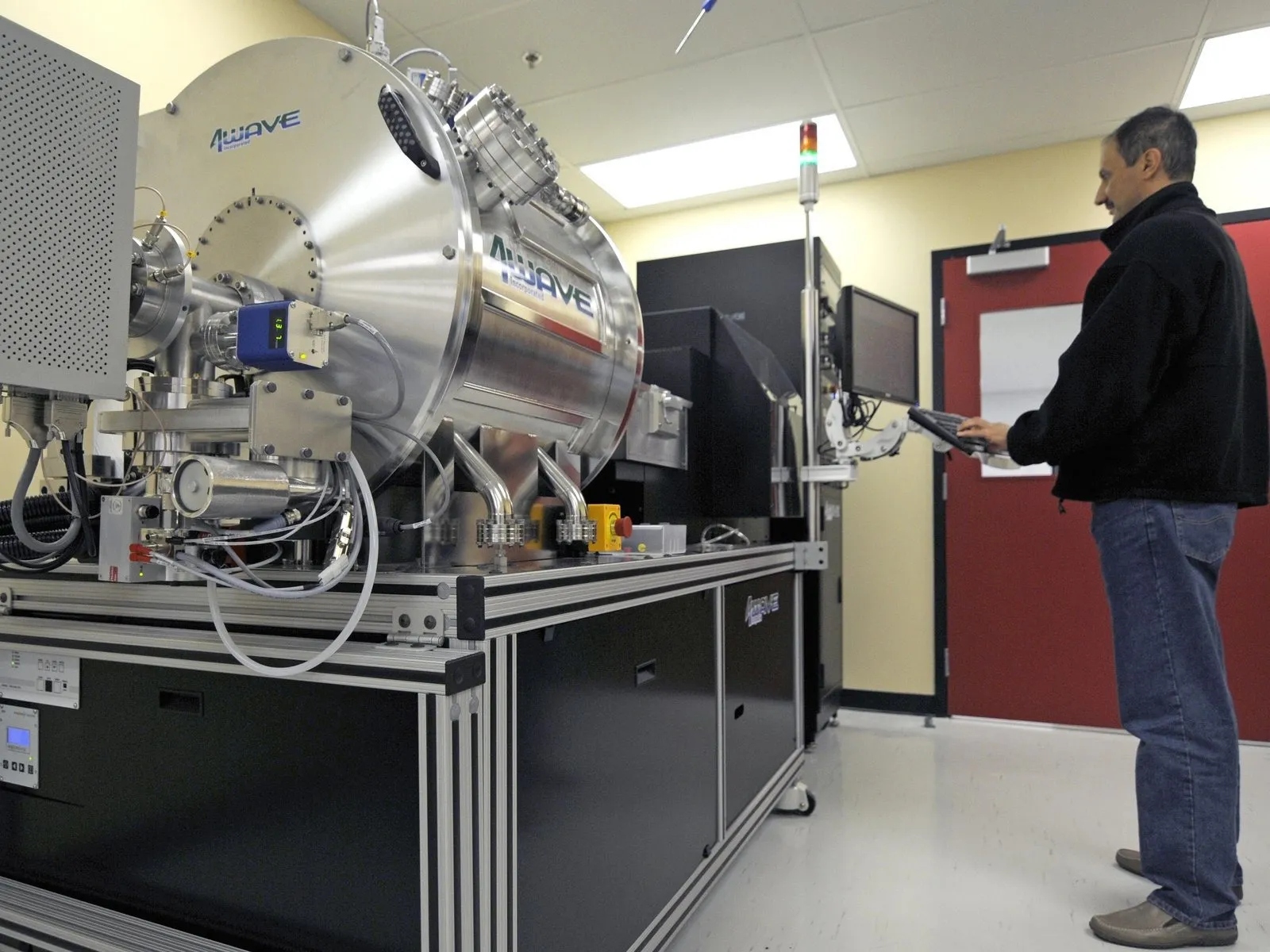
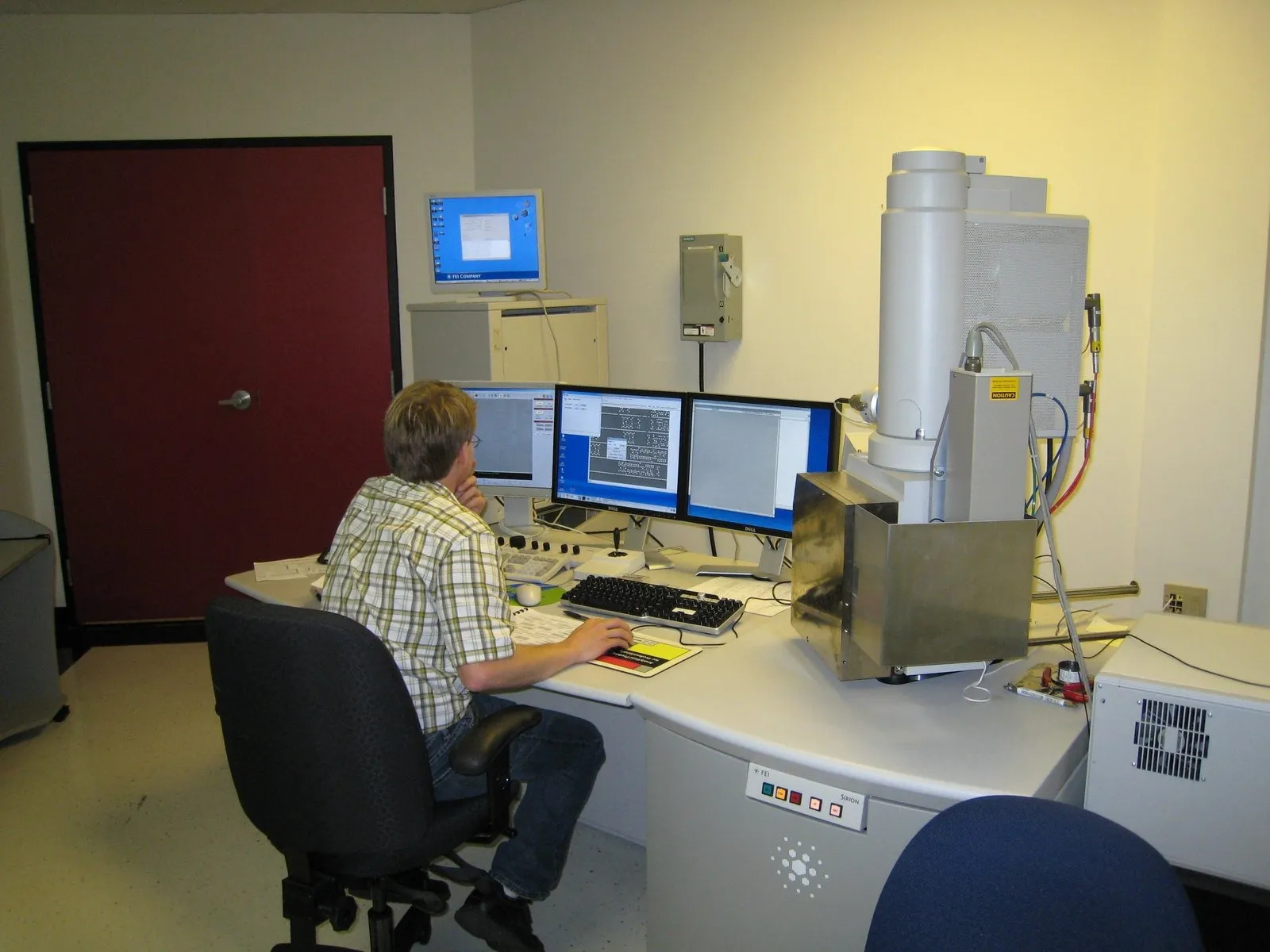
Using a microscope, Chipworks technicians capture images of the die by positioning it on an X-Y table controlled by a servo mechanism; laser monitoring ensures consistent focus throughout the imaging process.
The system incorporates programmed image positioning data, enabling automated die movement and capture of multiple images that are subsequently combined into a complete die photograph.
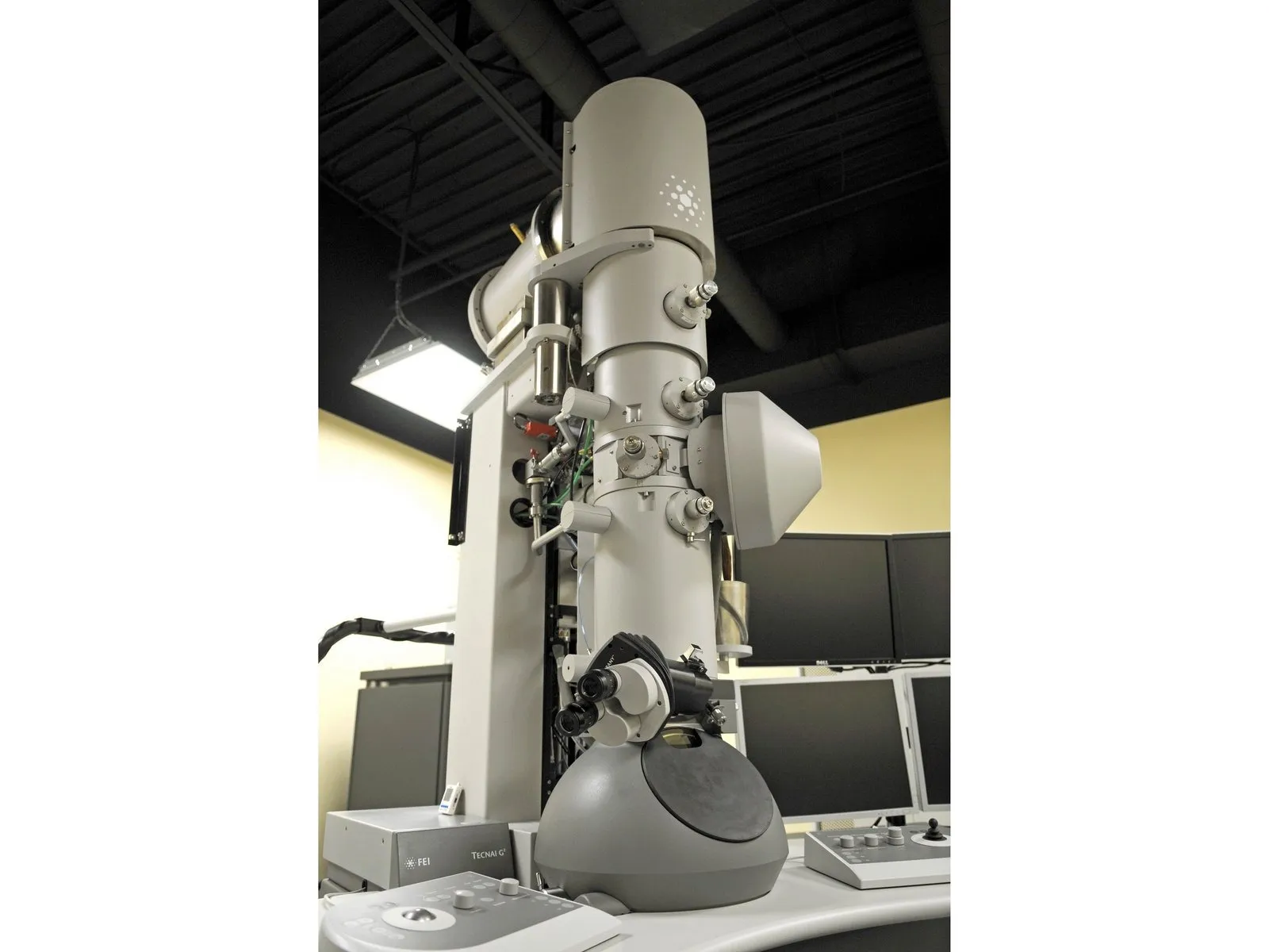
Refer to the third image to identify a machine utilized within the process.
The exposed surface of an A6 processor's metal die closely resembles the shape and appearance of a Wheat Thin cracker.
Chipworks employed a detailed process, beginning with photographing a single Wheat Thin.
To remove the A6 component's protective casing, immerse it in a heated solution of fuming sulfuric acid, maintaining a temperature optimized for effective decapsulation.
Using a microscope, Chipworks technicians capture images of the die by positioning it on an X-Y table controlled by a servo mechanism; laser monitoring ensures consistent focus throughout the imaging process.
The system incorporates programmed image positioning data, enabling automated die movement and capture of multiple images that are subsequently combined into a complete die photograph.
Refer to the third image to identify a machine utilized within the process.
Step 9
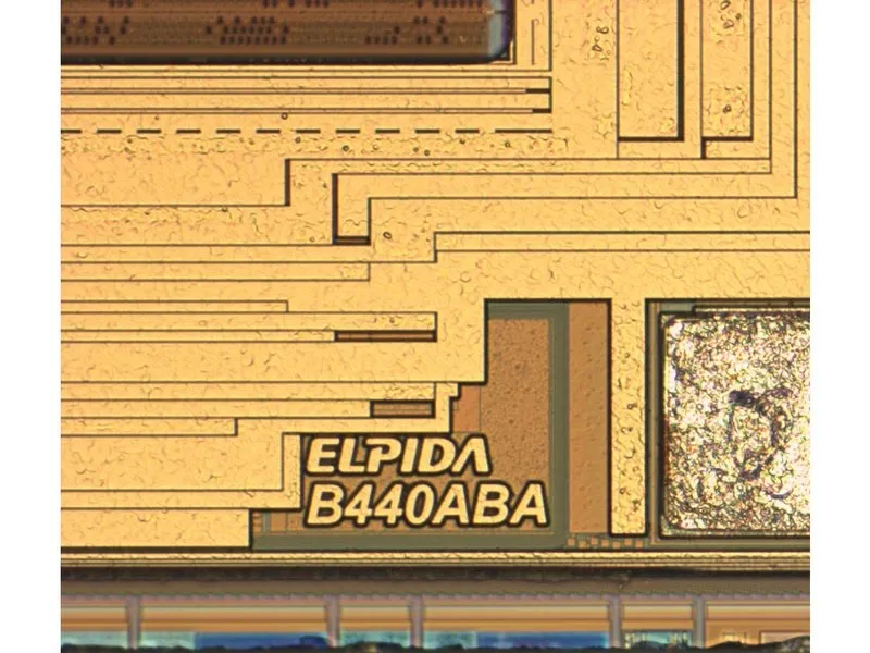
The iPhone 5's internal components include 1GB of Elpida LP DDR2 SDRAM, identifiable by the B8164B3PM silkscreen marking.
Analysis of the stamped identification on the memory module (as shown in the first image) alongside a photographic record of the marking (second image) strongly suggests Elpida manufactured the A6’s 1GB of low-power Double Data Rate 2 Synchronous Dynamic Random Access Memory.
Analysis by Chipworks identified the Elpida EDB8164B3 memory chip within the Motorola Droid RAZR Maxx.
Step 10
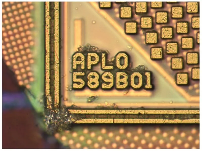
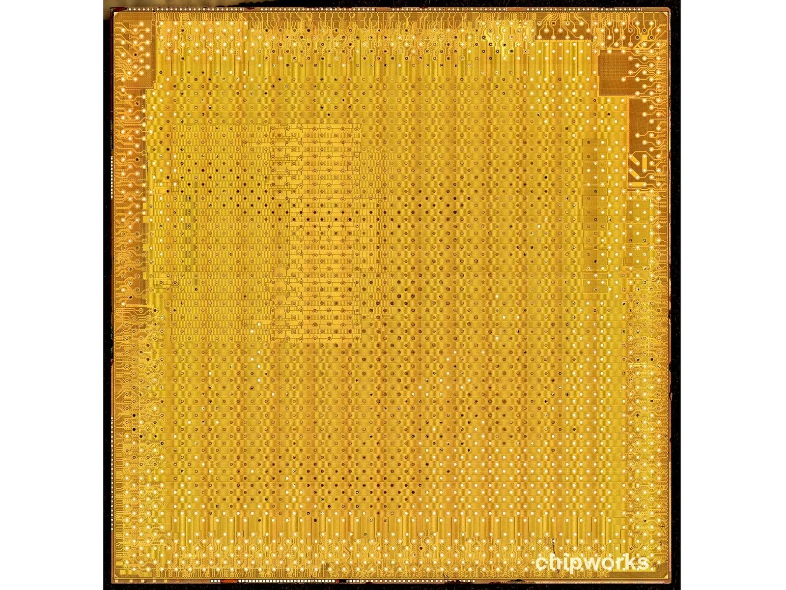
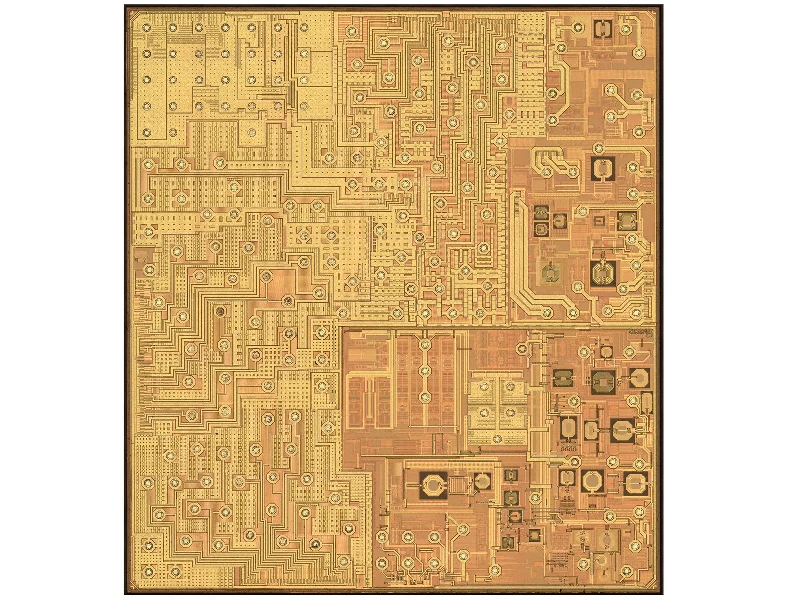
Despite being an Apple-branded A6 (APL0598, as indicated on the external packaging and APL0589B01 internally), this chip was manufactured by Samsung using their 32 nm CMOS process, with dimensions of 9.97 mm by 9.70 mm.
Apple's initial custom processor, the A6, while produced by Samsung, utilized Apple's design and operates on the ARMv7s instruction set.
Apple’s processor design authority enabled them to optimize its operation and characteristics according to their specific requirements.
Because the A6 die occupies 96.71 square millimeters, significantly exceeding the 70 square millimeter size of the prior Apple A5, a Samsung-manufactured chip built on a 32 nm HKMG process, it’s likely that the A6 incorporates substantially more features, assuming it also utilizes a 32 nm fabrication process.
Step 11
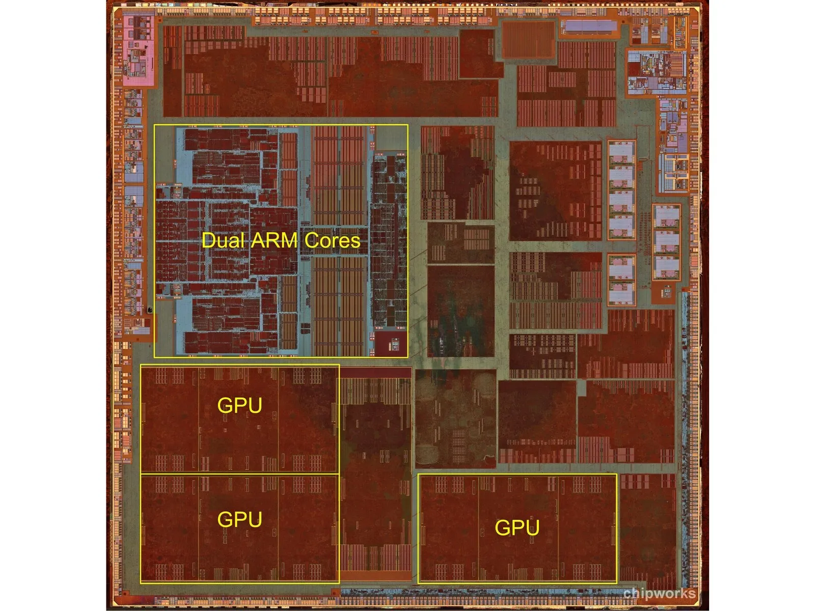
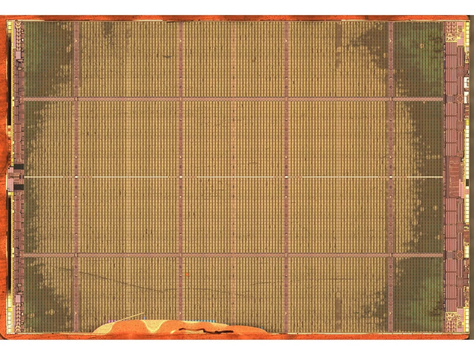
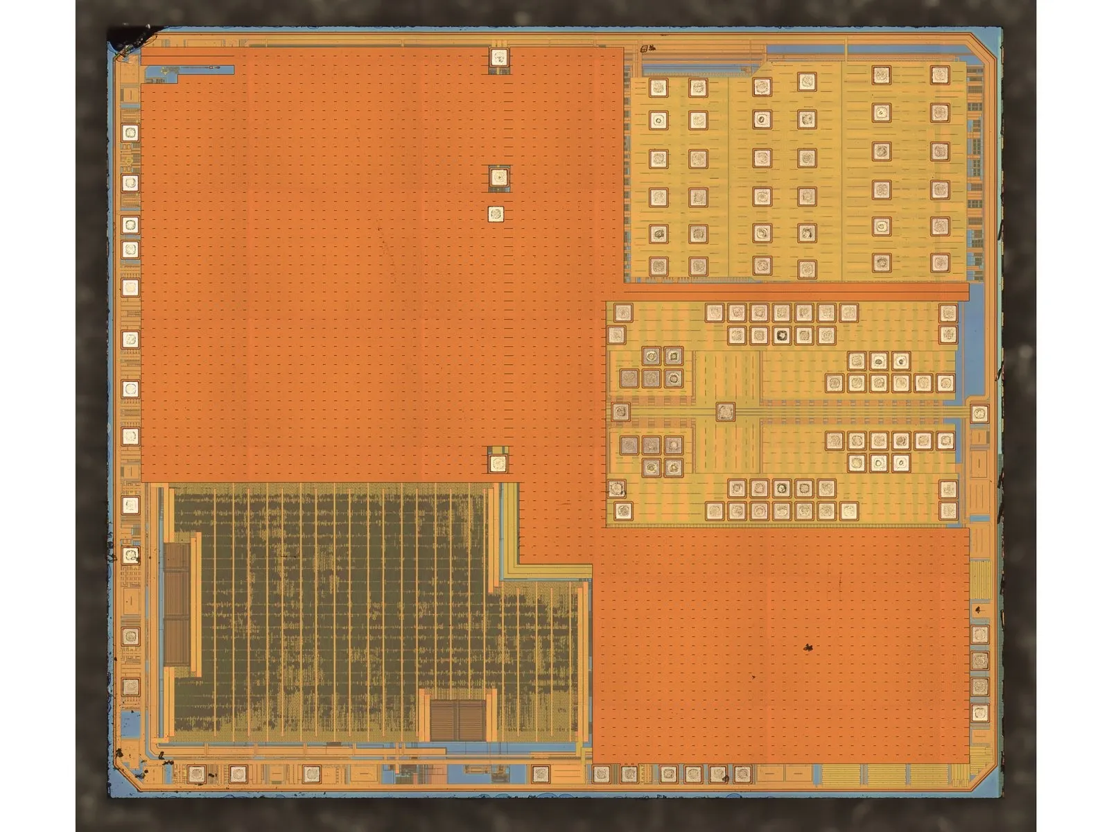
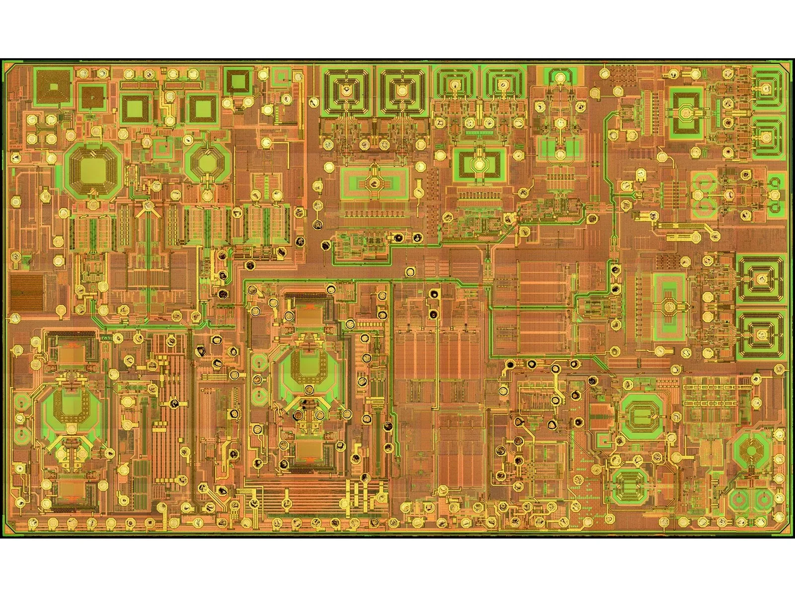
Within the A6 processor, locate the central area, where you will find the two ARM processing cores and the three PowerVR graphics cores.
Initially, the arrangement of the ARM cores appears less structured and streamlined than the GPU cores situated underneath, due to the GPU's more organized design.
Typically, specialized software automatically arranges logic blocks; however, the ARM core blocks appear to have been positioned manually.
Achieving quicker data processing is typically possible with a manual layout, though this approach demands significantly more time and incurs higher costs.
Due to the architectural design of ARM processors, speculation persists that Apple developed a processor with comparable performance to the latest Cortex-A15, representing a rare instance of a manually designed chip likely to be released in the coming years.
Step 12
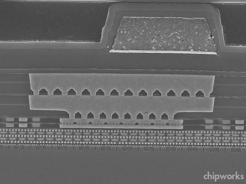
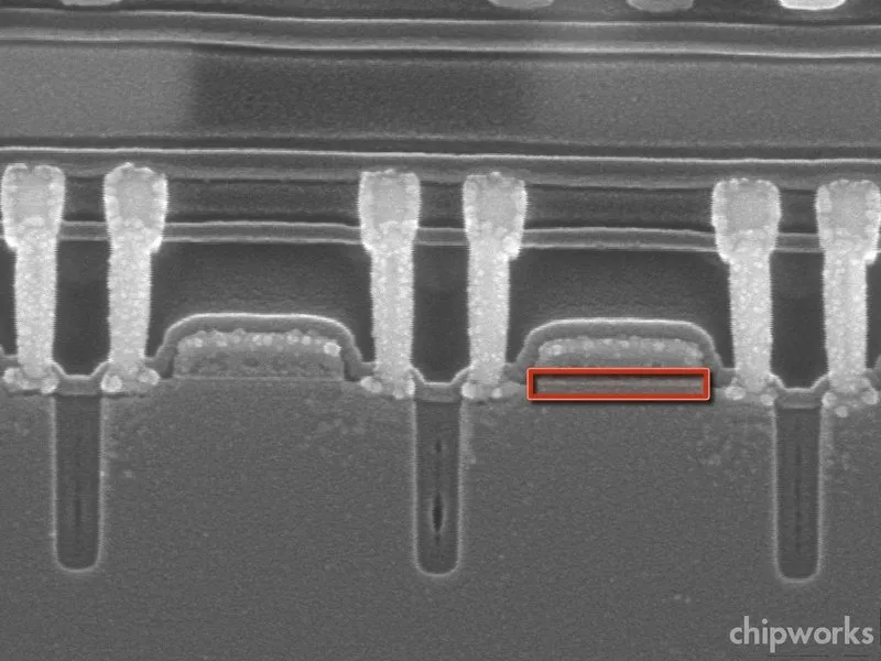
Examining the magnified cross-sectional image (second image), the distinct, elevated formations represent the transistors' internal architecture, while the small, connecting protrusions situated between these structures function as the electrical contacts linking the various layers.
The arrangement of transistors on the integrated circuit bears a striking resemblance to the design of ancient Roman aqueducts.
The presence of this extremely narrow feature indicates the semiconductor utilizes a 32 nanometer High-K Metal Gate manufacturing process.
The fabrication process for the A6 chip, employing 32 High-K Metal Gate technology, mirrors that found in the Apple TV 3rd Generation, specifically the APL2498 chip as documented by Chipworks.
The layer situated between the gate electrode and the silicon within a Field Effect Transistor possesses a dielectric constant, represented by the variable K, which is an inherent material property influencing the transistor's turn-on voltage.
Step 13 | Other Notable Chips
Despite the A6 chip's presence, the iPhone's operation relies on numerous additional integrated circuits that warrant detailed examination.
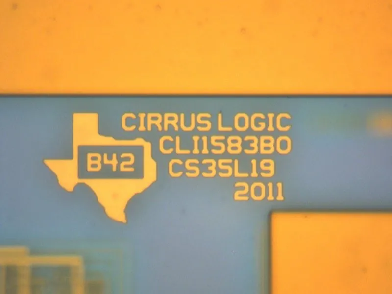
Analysis by Chipworks revealed the Apple 338S1077 utilizes a Cirrus CS35L19 integrated circuit, classified as a class-D audio amplifier.
Based on the inscription visible in the second image, the component appears to be a member of the CS35L family, likely the CS35L19 die, despite not being explicitly documented on the Cirrus website.
Step 14
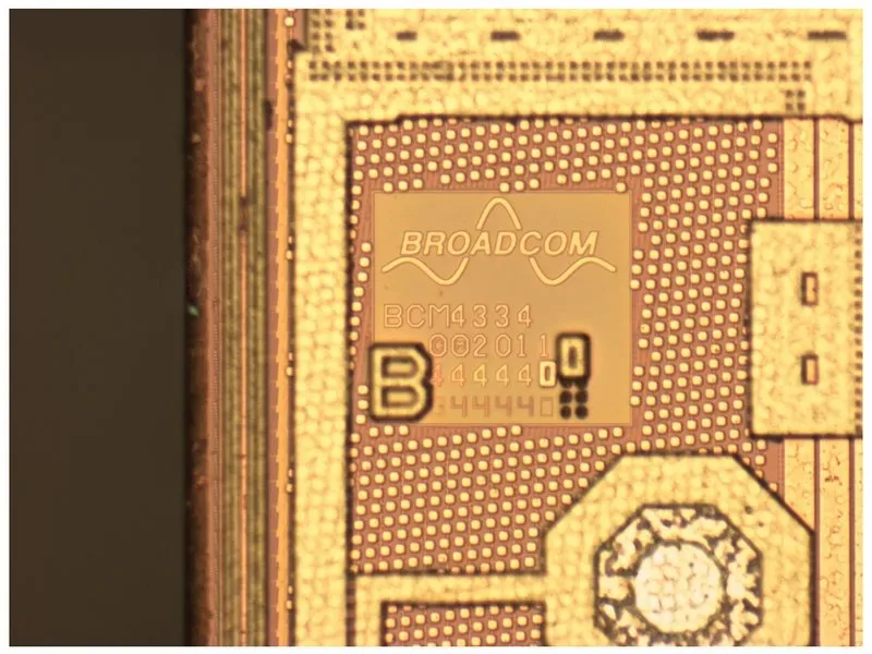
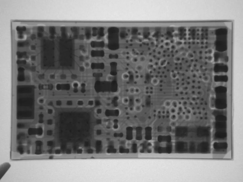
The Murata Wi-Fi SoC module incorporates a Broadcom BCM4334 package alongside an oscillator, capacitors, resistors, and other supporting components, as detailed in the X-ray image provided.
Murata manufactures a component housing that incorporates parts from other suppliers, then delivers the assembled unit to Foxconn for integration onto the iPhone’s logic board; Chipworks accurately described this process as Murata providing a structure containing components produced by other companies.
The Broadcom BCM4334 chip, manufactured in Taiwan by TSMC using a 40 nm CMOS process, includes these die images as reference material.
Wireless connectivity supports the 802.11 a, b, g, and n standards.
Compatible with Bluetooth version 4.0 High Speed.
Employ a frequency modulation receiver.
Step 15
The Qualcomm MDM9615 LTE modem and RTR8600 multi-band/mode RF transceiver assemblies are next; while the MDM9615 was previously detailed during the iPhone 5 disassembly, a summary follows.
The MDM9615 chip enables LTE connectivity with multiple spectrum bands and operating modes, facilitating concurrent voice and data transmission over LTE networks, contingent upon carrier infrastructure support.
To enable support for a range of frequencies, the MDM9615 works in conjunction with the Qualcomm RTR8600, a radio transceiver capable of multiple bands and modes, specifically encompassing 5 UMTS bands, more than 5 LTE bands, and 4 EDGE bands.
The diagram illustrates the procedure for this stage.
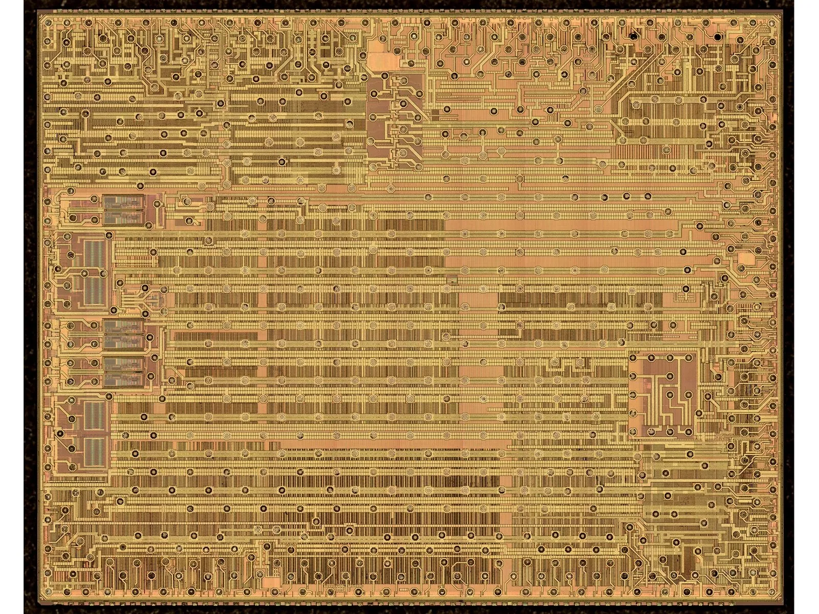
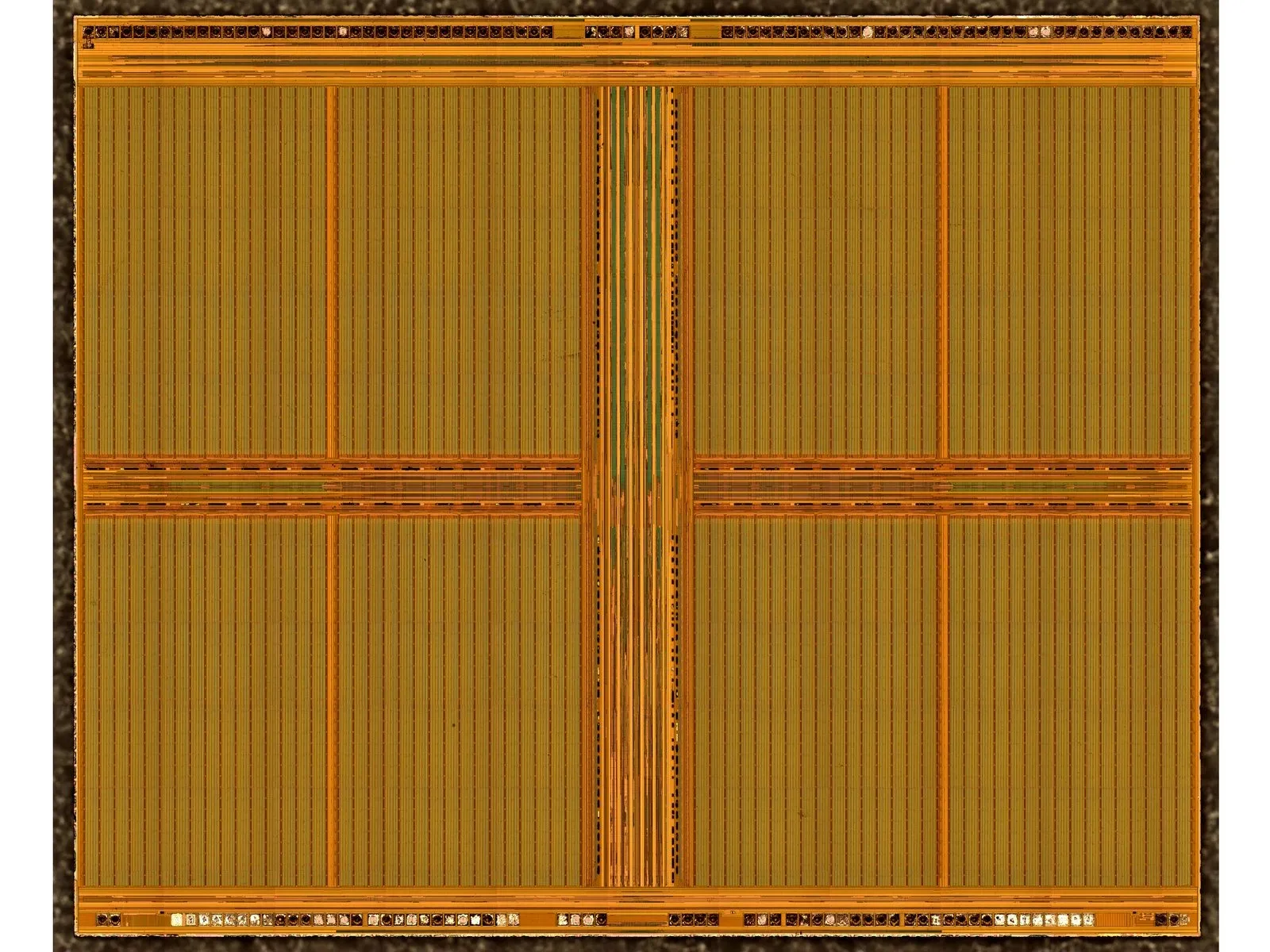
Refer to the initial illustration to view the HG11-N3877 LTE Baseband die.
The MDM9615 also utilizes a Samsung 1G-F-MC memory die, which has a capacity of 128 MB.
Refer to the third image for a view of the RTR8600 die.
The MDM9615 chip enables LTE connectivity with multiple spectrum bands and operating modes, facilitating concurrent voice and data transmission over LTE networks, contingent upon carrier infrastructure support.
To enable support for a range of frequencies, the MDM9615 works in conjunction with the Qualcomm RTR8600, a radio transceiver capable of multiple bands and modes, specifically encompassing 5 UMTS bands, more than 5 LTE bands, and 4 EDGE bands.
The diagram illustrates the procedure for this stage.
Refer to the initial illustration to view the HG11-N3877 LTE Baseband die.
The MDM9615 also utilizes a Samsung 1G-F-MC memory die, which has a capacity of 128 MB.
Refer to the third image for a view of the RTR8600 die.
Step 16

We appreciate Chipworks' collaboration, which provided valuable access to their facilities and revealed the iPhone 5's unexpectedly straightforward repair process.
Further examination of iPhone 5 packaging reveals significant differences, leading experts to conclude that the device represents a completely new design, rather than a progression from previous models, despite superficial similarities.