Fix iPhone X Unable to Activate By Jumper Wires
Prior to commencing any repair work, disconnect the device completely from all electrical power.
- To complete this repair, you will need the following tools:Use a Phillips head screwdriver.
Should problems arise while performing the repair, refer to the manufacturer's published materials or obtain help from a qualified technician.
Step 1 | Jumper Wires
- Following a drop, the iPhone X is experiencing operational failure, and subsequent restoration attempts have resulted in an inability to activate the device.
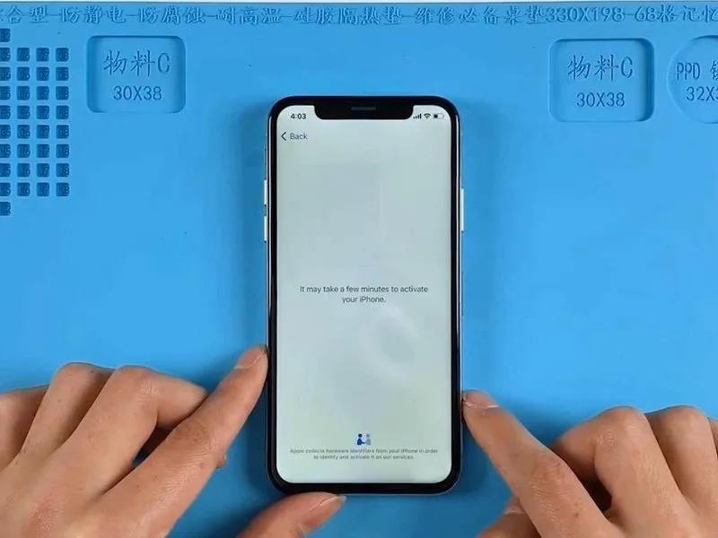
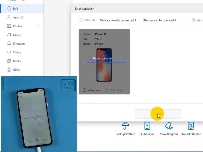
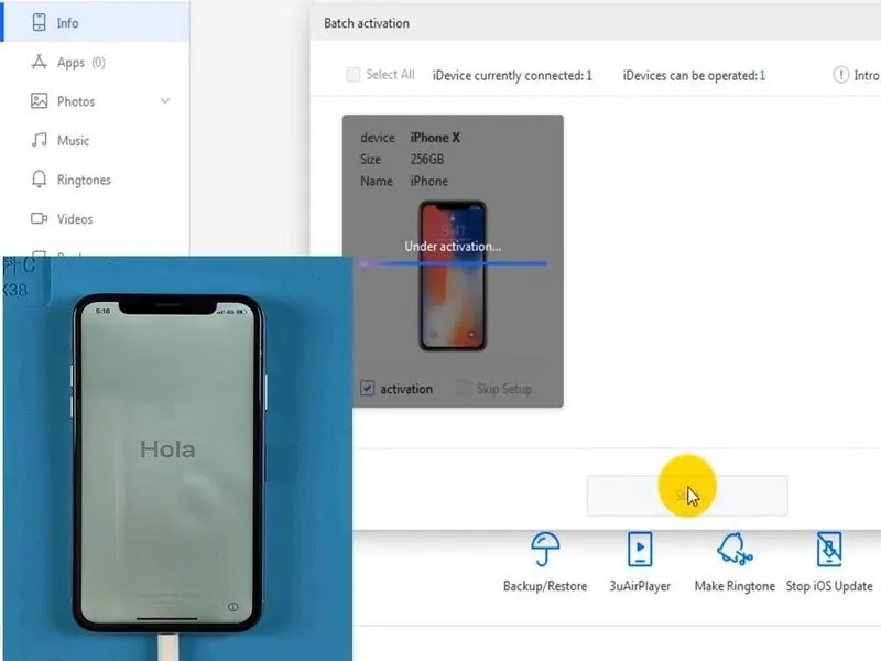
- Using the appropriate software and following the on-screen prompts, attempt to power on the device.Employ the 3uTools software..
Establish a data connection between the mobile device and the computer, then launchUtilize the 3uTools software.Initiate the activation process and begin by selecting the "Activate Now" button.
Following initiation, the activation process typically requires multiple minutes; however, if the device remains within the activation interface for approximately 20 minutes, activation will fail.
Step 2
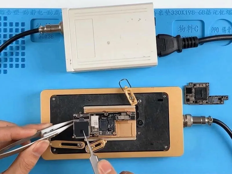
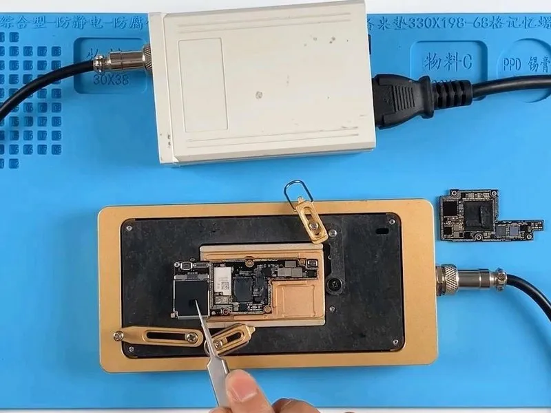
- Carefully detach the motherboard from the chassis to allow for a more detailed inspection.
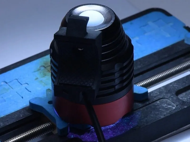
Carefully position the motherboard onto.The heating platform's operating temperature is 165 degrees Celsius.Bring the temperature up to the specified level.A temperature of 165 degrees Celsius is required.Using tweezers, carefully detach the logic board and signal board.
Step 3


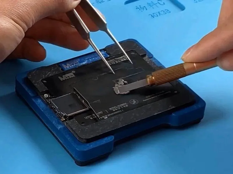
- Using a Sculpture Knife, carefully remove all traces of the thermal grease.
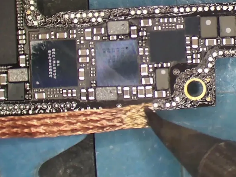
Following disassembly, a significant number of pads are observed to be absent; these should be reconstructed by soldering jumper wires to bridge the gaps.
Using the holder, secure the logic board and then eliminate the solder residue from the bonding pad with flux remover.Employ a soldering iron heated to 365 degrees Celsius.Using appropriate safety precautions, ensure the 1/4-inch hex wrench is fully inserted into the retaining screw, then rotate it 90 degrees clockwise to release the component.Utilize desoldering braid to remove excess solder..
Step 4

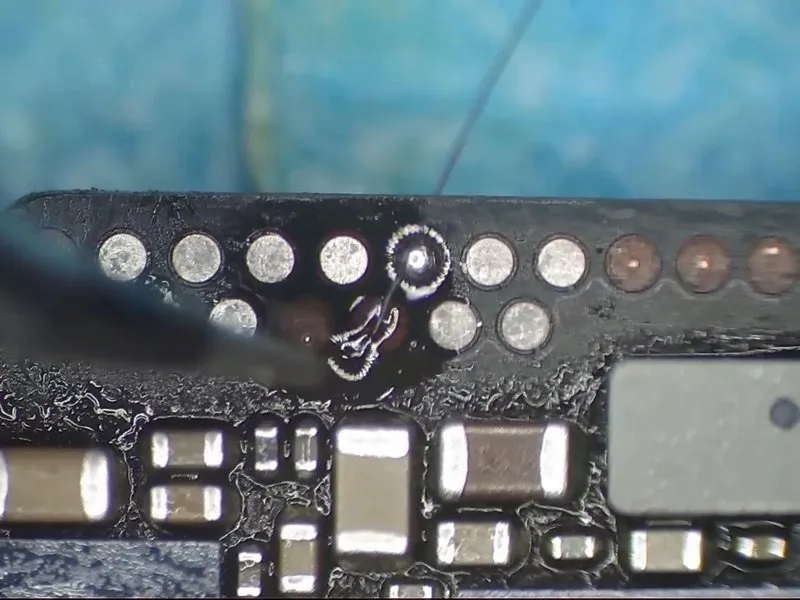

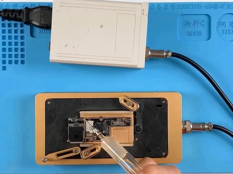
- Using a hot air gun, reflow solder paste onto the absent pads to create a solder joint.A temperature of 340 degrees Celsius is required.Using PCB Cleaner, thoroughly remove any contaminants from the bonding pad, then apply a thin layer of Paste Flux.
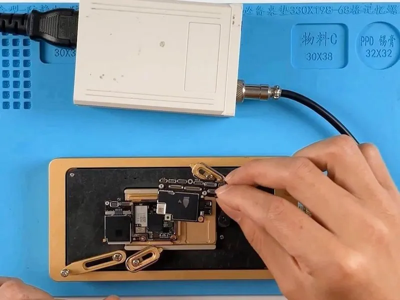
Employ soldering to connect 0.02 mm copper wires to the bonding pad.Utilize a soldering iron.Ensure a secure, soldered connection for all copper wiring.
Using PCB Cleaner, thoroughly remove any remaining residue, then carefully shape the copper wires into the required pad formations with the aid of Tweezers and a Sculpture Knife.
Step 5
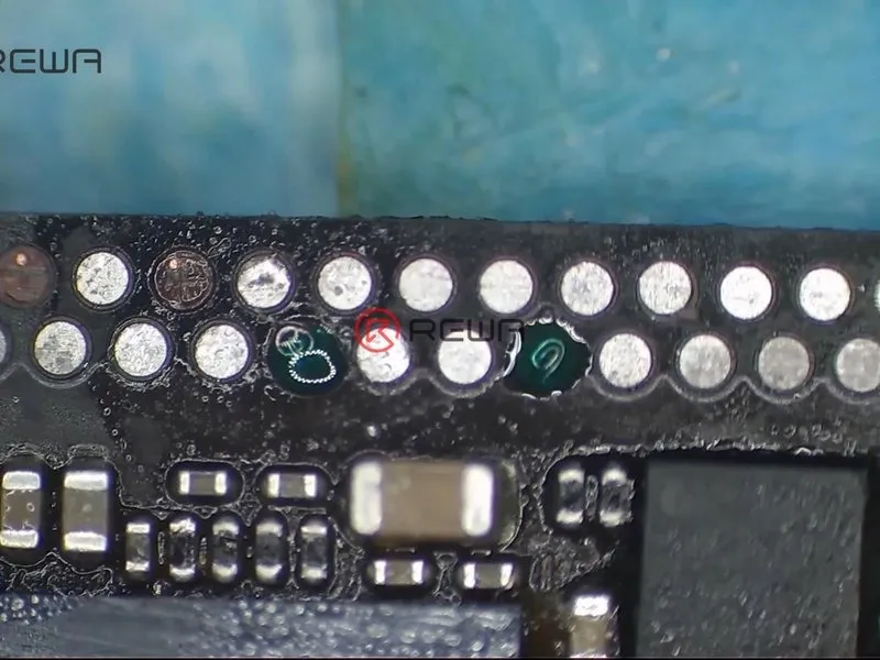
- Introduce the substance to the designated area.Apply solder mask material to all areas of the printed circuit board, excluding component pads and test points, ensuring a thickness of 1 mil and adhering to the manufacturer's recommended curing process.Secure the copper wires to the bonding pad, then cure the solder mask using a UV lamp for a duration of 5 minutes.
- Carefully remove any surplus solder mask material using a blade.Employ a carving knife designed for sculpting.Expose the copper wiring.
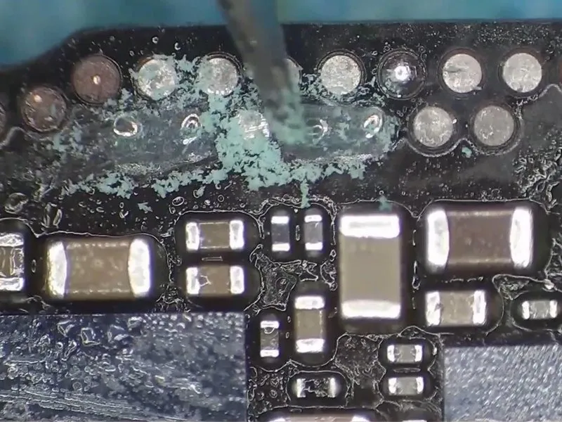
- Employ desoldering braid to eliminate excess solder from the bonding pad.Employ a soldering iron.Maintain a temperature of 365 degrees Celsius.Use desoldering braid to remove excess solder.Use a suitable solvent to remove any contaminants from the bonding pad.Use a cleaning solution specifically designed for printed circuit boards to remove contaminants..
Step 6


- Secure the signal board using the four 3.5mm screws, ensuring proper alignment before tightening.A reflow soldering station with a reballing template is required.Carefully align the reballing stencil over the target area.
- Position a metal plate to block solder paste migration during the soldering process, safeguarding the motherboard.
- Distribute a uniform coating of low-temperatureApply solder paste to the designated pads on the circuit board, ensuring a uniform layer approximately 0.020 inches thick, using a squeegee or stencil, and avoid applying excessive amounts that could cause bridging between components..
Step 7
- Heat the motherboard to a temperature of 165 degrees Celsius.The work surface is heated.Increase the temperature.
- Following formation of the solder balls, de-energize the circuit and allow the signal board to return to ambient temperature. Then, apply a thin layer of Paste Flux and carefully position the logic board in alignment with the signal board.
- Maintain the heating process for an additional 60 seconds once 165 degrees Celsius is achieved, then deactivate the power supply and allow the motherboard to return to ambient temperature.
Step 8
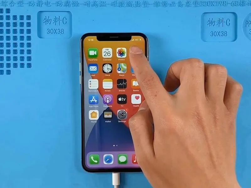
Carefully position and secure the motherboard within the phone's chassis.Utilize the 3uTools software.Successful activation of the device is confirmed.
Verify the operation of all remaining features; performance is satisfactory.