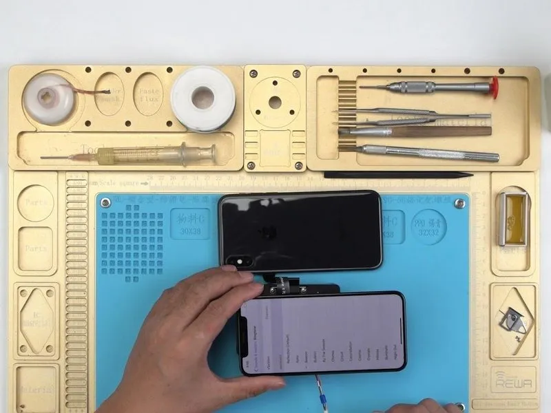
iPhone X Bottom Speaker Repair
Prior to commencing any repair work, it is essential to disconnect the device entirely from all electrical power supplies.
- Necessary tools for this procedure include:A Phillips head screwdriver is needed.
For precise information regarding your particular model and supplementary safety guidelines, consult the device's user manual.
Step 1 | Speaker

- The device exhibits a cracked screen and a physically damaged casing; a replacement display assembly is required, followed by a functional test. The device powers on without issue, and both the front-facing and rear cameras operate as expected, alongside proper WiFi connectivity.
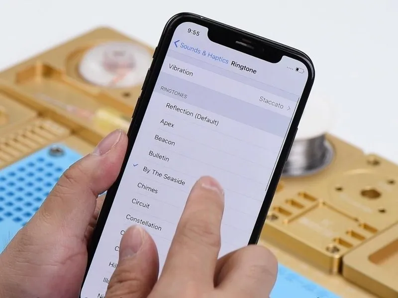
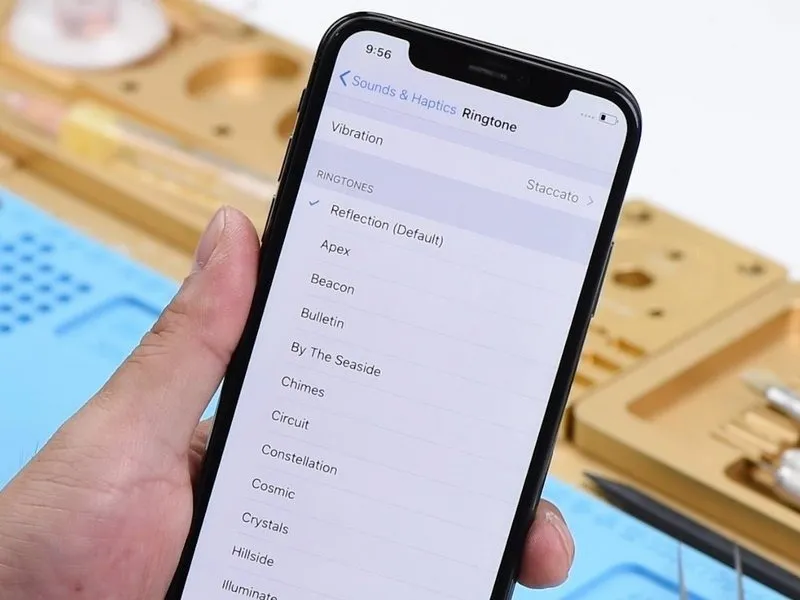
- Navigate to the Sounds & Haptics menu, then select Ringtone. Choosing a standard ringtone produces no audible output; however, sound is functional when headphones are connected.
- Based on initial assessment, the audio circuitry appears to be operating correctly; the issue appears to be limited to the failure of the bottom speaker. To proceed with troubleshooting, remove the display assembly and detach the battery.
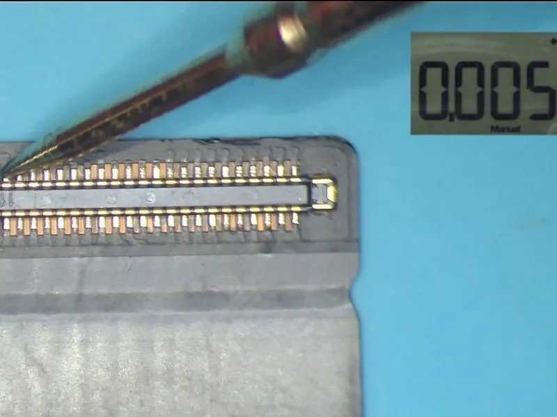
- Separate the charging port flex cable and perform a diode mode test on pins 1 and 45 of the DOCK connector. The measured resistance is5, confirming the bottom speaker's functionality.
Step 2
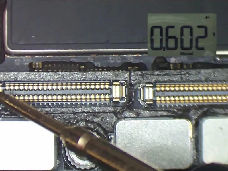

- Proceed with assessing the voltage levels at Pin 1 and Pin 45 on the motherboard's J6400 connector.The voltage reading obtained from Pin 45 registers as 602 millivolts, indicating a standard operational level.However, the voltage measurement at Pin 1 displays as 'Over Limit' (OL), signifying a deviation from expected parameters.
- This 'Over Limit' reading on Pin 1 suggests a potential malfunction requiring further investigation.
Step 3

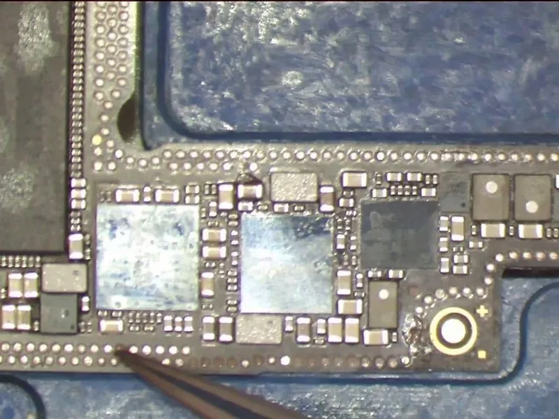
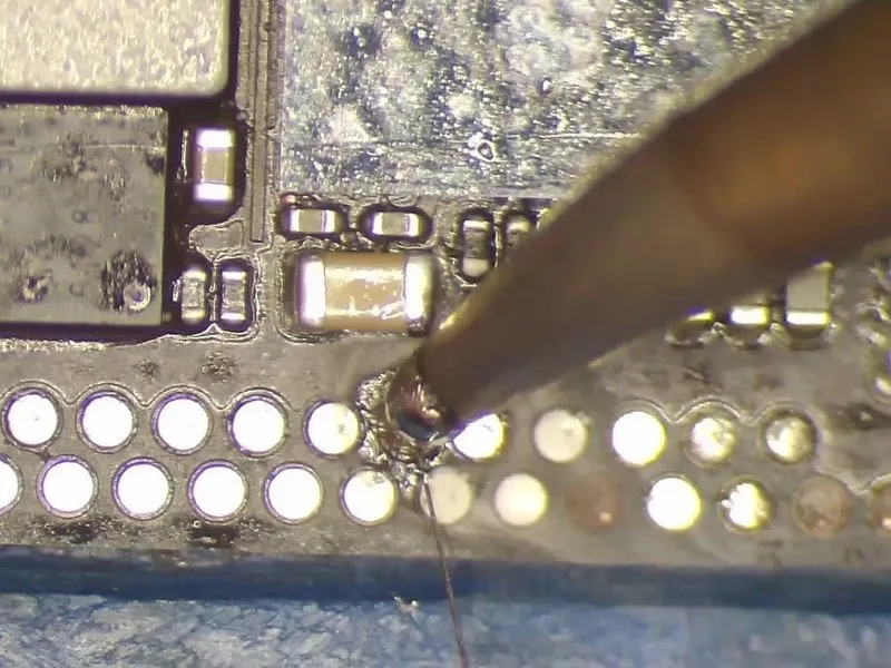
The observed behavior indicates a break in the circuit associated with Pin 1, suggesting an open connection. Specifically, Pin 1 of connector J6400 establishes a connection to Pin 2 of the speaker amplifier integrated circuit, U4900, utilizing Pin S162 located on the cylindrical components situated around the perimeter of the lower circuit board layer.
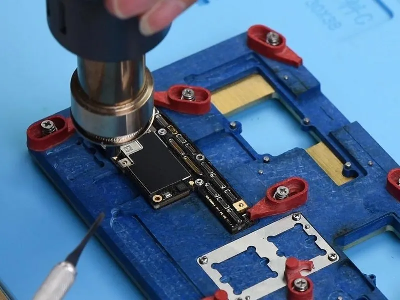
The subsequent diagnostic step involves a meticulous inspection of the circuit path. To facilitate this, disconnect the flexible cables connected to the motherboard and remove the motherboard from the device. Secure the motherboard to the designated Holder. Apply heat using a Hot Air Gun, maintaining a temperature of360°C, and a regulated airflow of 65.
Step 4

After a sixty-second interval, carefully lift the uppermost layer incrementally. Observe that the adhesive securing the cylindrical components has fully liquefied to ensure proper separation; timing is critical for successful detachment. A visual inspection reveals several absent pins on the upper layer, specifically PinS166 belonging to the NFC circuit.
Step 5
- The device's condition suggests a drop impact occurred, leading to an unintended bonding of the motherboard's solder joints and subsequent pin displacement. Although several detached pins are ground connections and can be disregarded, Pin S166 necessitates repair through jumper wiring.
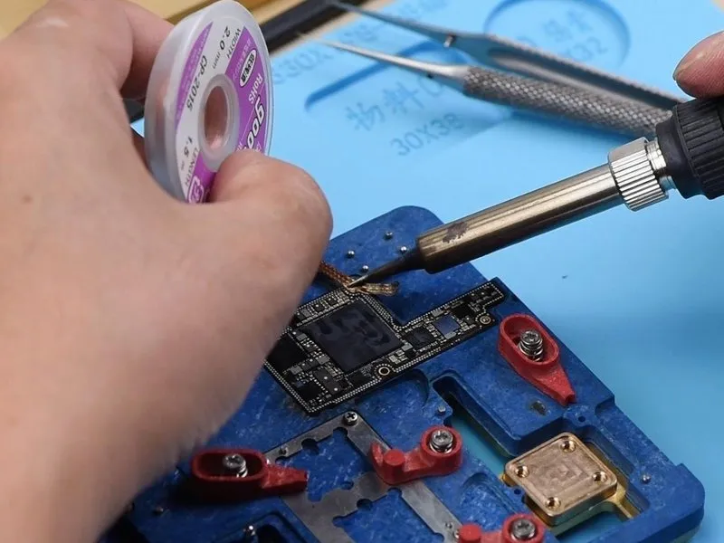
- Employing a rosin-saturated Solder Wick, eliminate excess solder from the perimeter of the lower layer's cylinders and the upper layer's bonding pads.Solder WickFollowing the desoldering process, utilize PCB Cleaner to ensure a clean surface.
Step 6
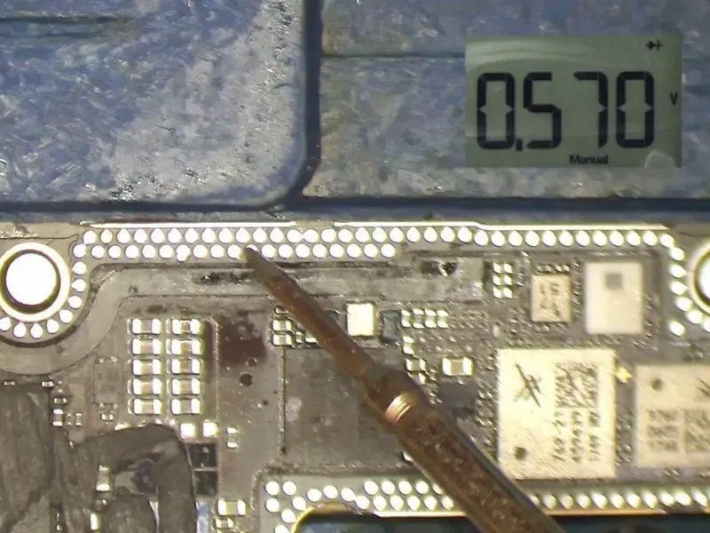


- Perform a diode mode test on Pin S162, associated with the cylinders, and confirm a reading of 570 millivolts, indicating a standard result.
Proceed with measuring Pin S163, also observing a typical value of 570 millivolts.
Based on these observations, the open circuit affecting Pin 1's circuitry is likely due to inadequate solder joints around the perimeter of the lower layer, specifically on the cylinders. - Secure the motherboard within the testing apparatus, ensuring the display assembly's extension flex cable is properly fastened.
Subsequently, connect the display assembly and the charging port flex cable. - Establish a connection between the battery connector and the DC Power Supply; utilize tweezers to momentarily bridge Pin 9 of connector J4300 to ground.
This action will simulate a power button press, and the ammeter should display a standard current reading.
Step 7

- Navigate to the device's Settings menu, then proceed to Sounds & Haptics, and finally select Ringtone.
Choose a standard ringtone and ensure the audio output is functioning correctly during this test. - Verification at this stage should confirm the integrity of both the upper and lower layers.
The root cause of the malfunction stems from inadequate or incomplete soldering connections on the cylinders.
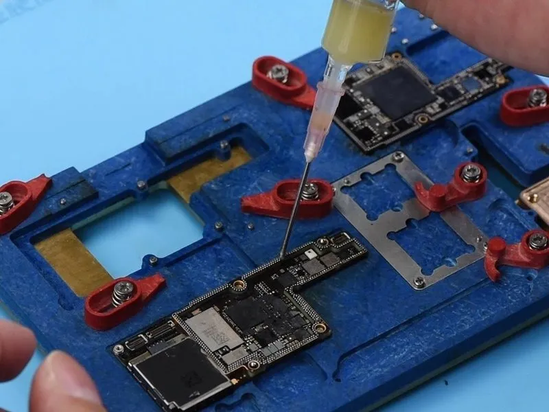
To resolve this issue, a secure bond must be established by soldering the two layers together; additionally, jumper wiring is required to address Pin S166 prior to the soldering process. - Apply solder material to the Via using aSoldering Ironheated to a temperature of 360°C.
Acquire a length of Enameled Copper Wire with a diameter of 0.02mm, and ensure it is pre-coated with solder.
Securely attach one end of the prepared wire to the solder-covered Via.
Step 8
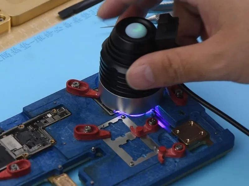

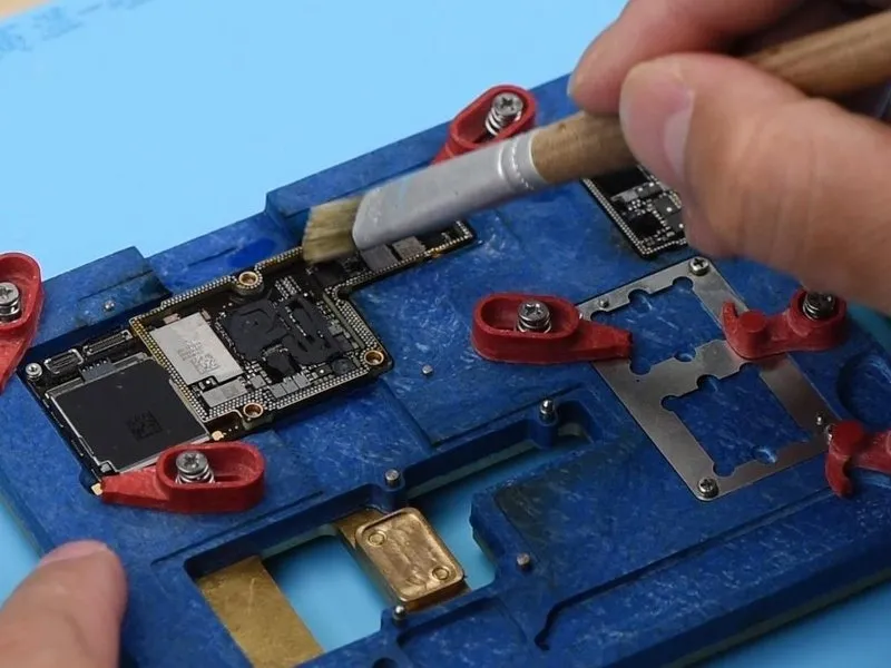
- Following the repair, utilize a PCB cleaner to remove any residue.
Subsequently, apply a UV curable solder mask to the area where soldering occurred.
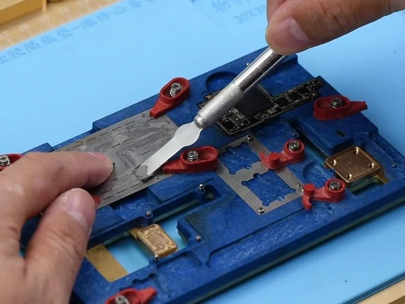
Allow the upper layer to harden beneath a UV dryer lamp for a duration of 2 minutes. - Carefully position the opposite end to its designated location.
Following that, secure the lower layer to the PCB holder.
Ensure the BGA reballing stencil is precisely aligned.
Distribute Soldering Pasteuniformly across the BGA reballing stencil using a BGA Scraper.
Eliminate any surplus Soldering Paste with a lint-free cloth. - Apply heat consistently with a Hot Air Gun, maintaining a temperature of 350°C and an airflow rate of 35.
This ensures that all solder balls achieve complete solidification.
After a waiting period of 2 minutes, detach the BGA reballing stencil.
Reapply heat with a Hot Air Gun to guarantee proper solder ball formation.
Step 9

- Introduce a quantity ofBGA Paste Fluxto the cylinder perimeters, ensuring the upper layer is correctly situated.
- Distribute heat uniformly utilizing aHot Air Gunat a temperature of350°C, with an airflow rate of 65.
Successful completion of the soldering procedure is indicated by the upper layer settling andPaste Fluxextruding outwards. - Allow the motherboard to undergo a cooling period of 5 minutes.
Proceed with phone reassembly and subsequent testing; navigate toSettings>Sounds&Haptics>Ringtone.
Choose a standard ringtone, verifying normal audio output.