iPhone X Teardown
A decade prior, Apple unveiled the pioneering iPhone, fundamentally reshaping the technological landscape. Currently, we are disassembling Apple's eighteenth model—theiPhone X. Featuring curved borders and a display extending to the edges, we anticipate this embodies the iPhone envisioned by Steve Jobs years ago; however, now that his concept has materialized, its impact remains to be seen. The future will determine its significance, but for the present, we aim to assist you in forming your own judgment. Accompany us as we explore Apple's flagship device to reveal its inner workings.
- Our sincere gratitude goes toCircuitwise for providing the location for our teardown in Australia,
- Creative Electron for supplying the X-ray images,
- andTechInsights for identifying the integrated circuits.
The timing is fortunate that we are in Sydney, coinciding with the opening of our Australian retail location. As our understanding deepens, we will share updates on Facebook, Instagram, and Twitter. We also offer a newsletter for those who prefer email communication.
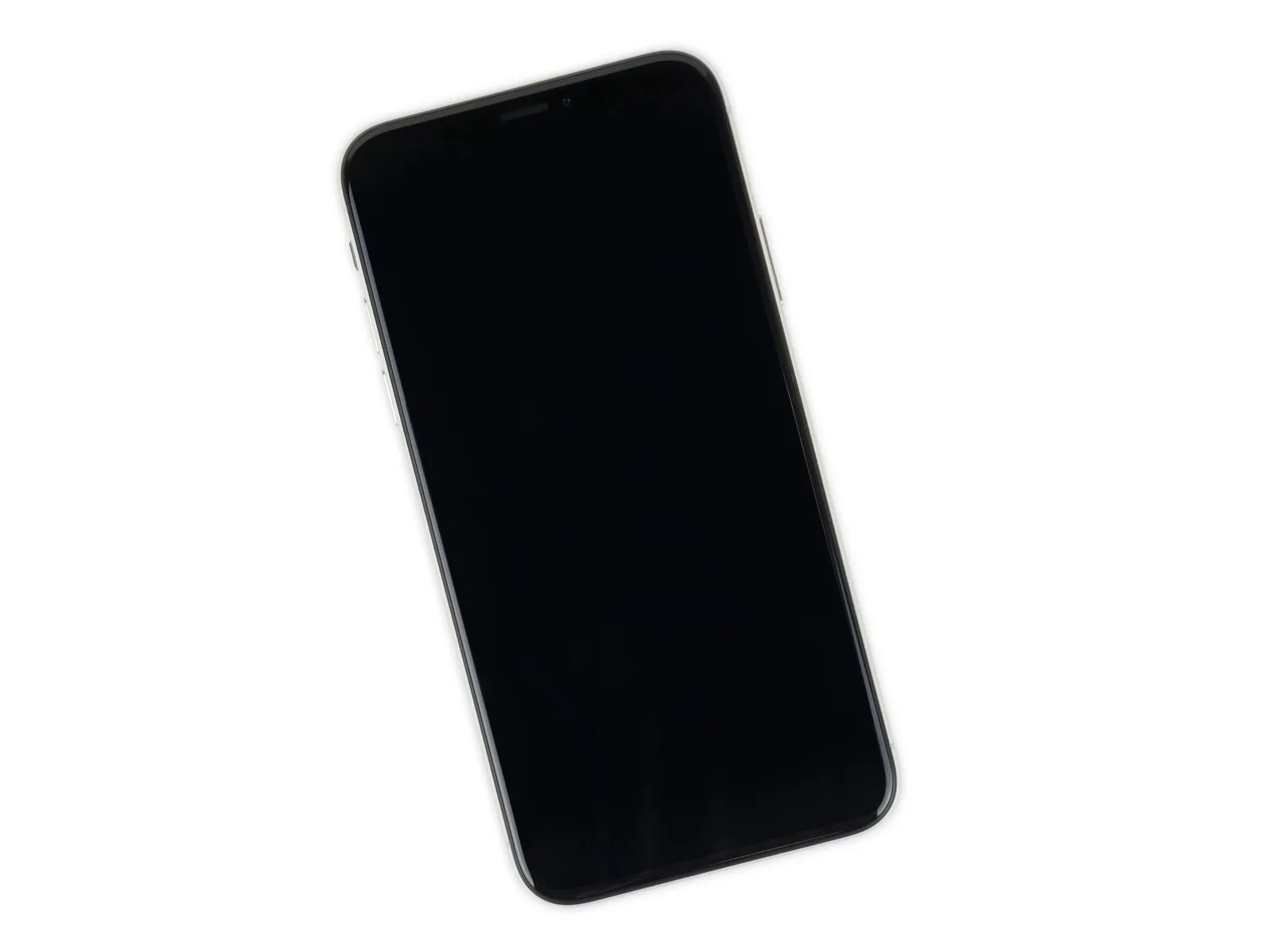
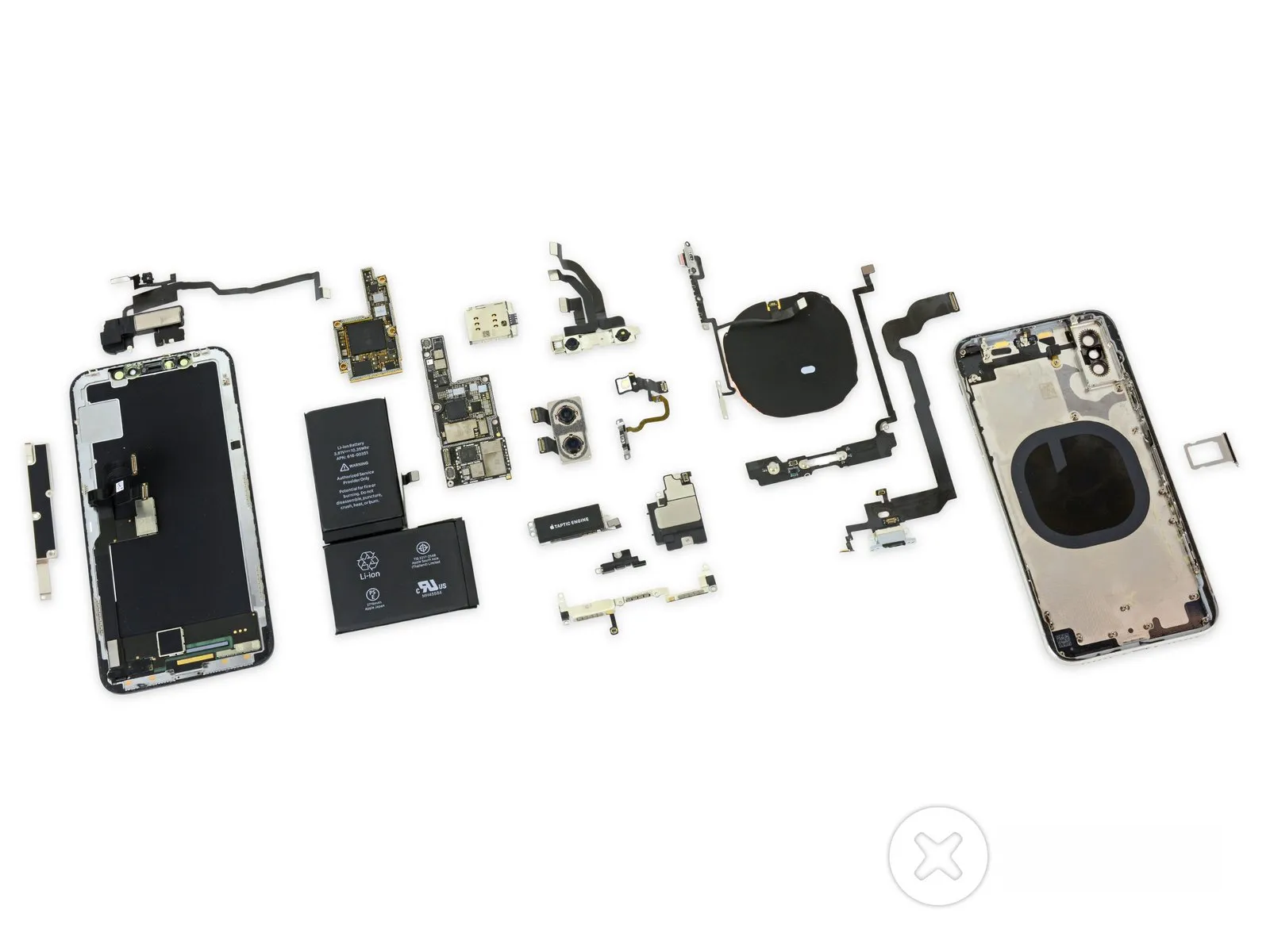
Step 1 | iPhone X Teardown

- Model A11features a Bionicprocessor, integrating a neural engine and a dedicated M11 motion coprocessor.
- The device incorporates a 5.8-inchimmersive, all-screen OLED multitouch Super Retina HD display, boasting a resolution of 2436 × 1125 pixels and a pixel density of 458 pixels per inch.
- Photography capabilities include a dual camera system, comprised of 12-megapixelwide-angleandtelephotolenses, each with apertures of f/1.8 and f/2.4 respectively, and optical image stabilization.
- A 7-megapixel TrueDepth camera is also present, offering 1080p HD video recording and Face ID functionality, with an aperture of f/2.2.
- The device is compatible with both fast-charge technology and Qi wireless charging standards.
- Our A1865 global model provides extensive cellular network compatibility, alongside 802.11a/b/g/n/ac Wi-Fi with MIMO technology, Bluetooth version 5.0, and NFC capabilities.
Step 2
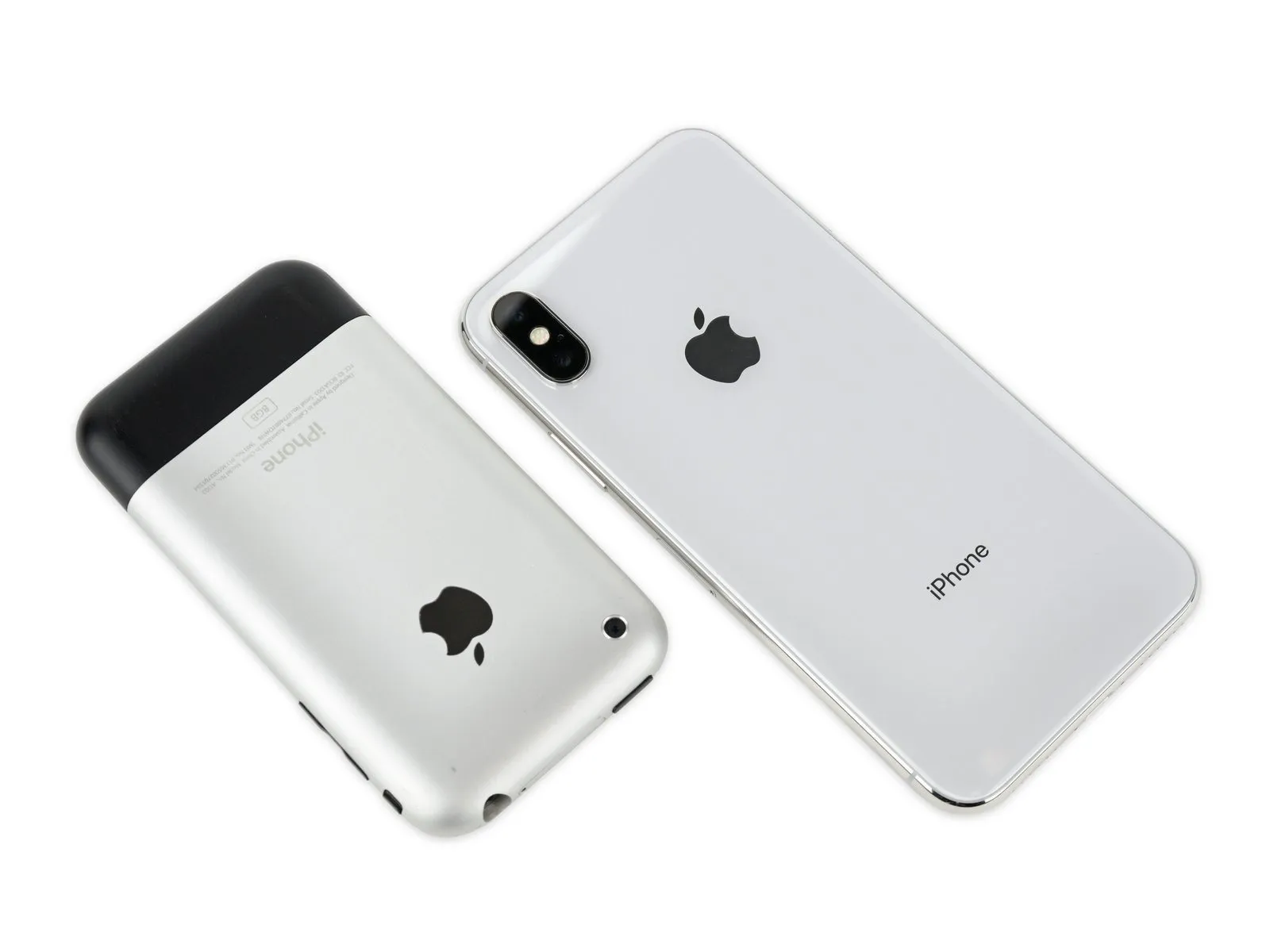
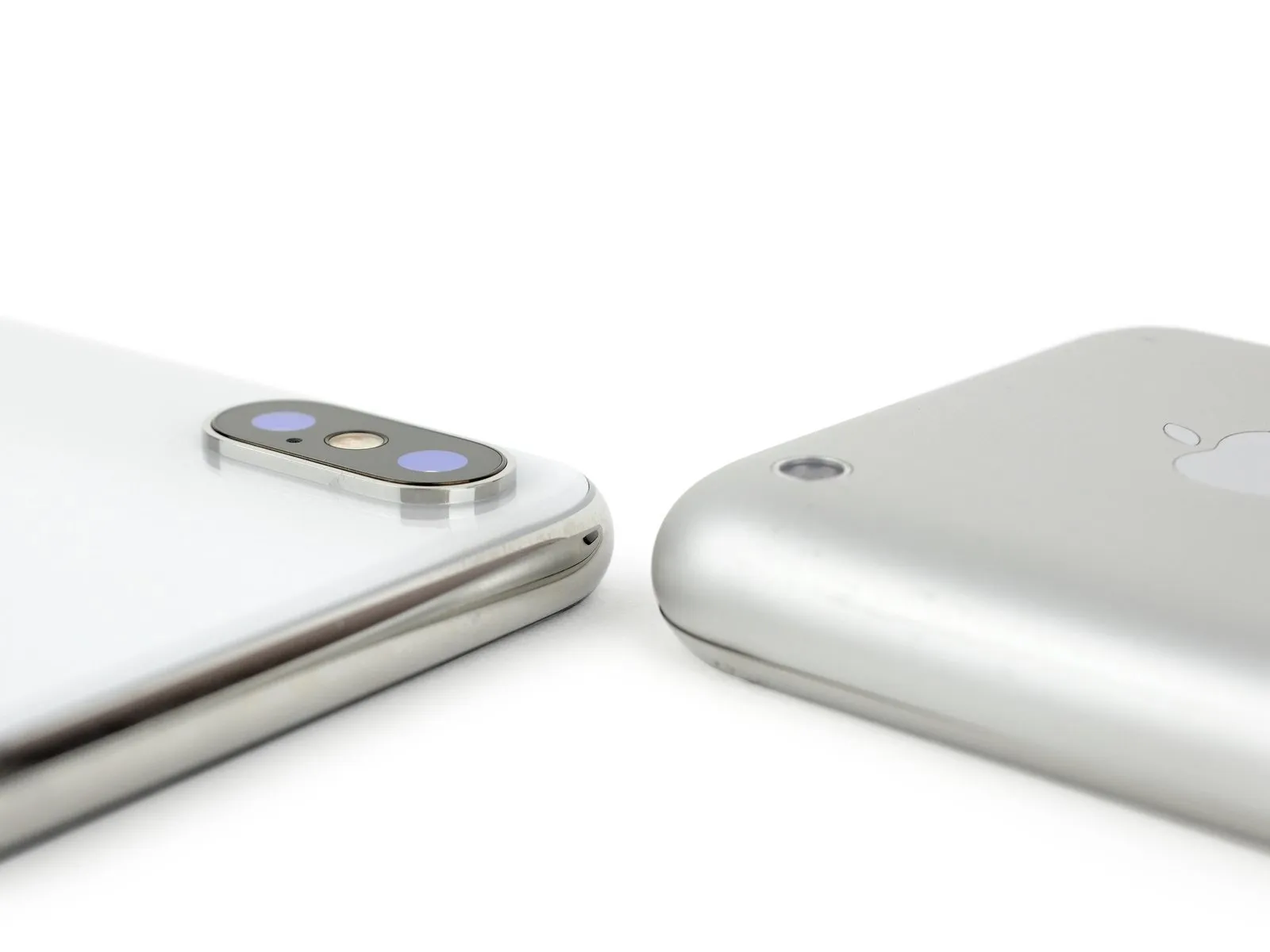
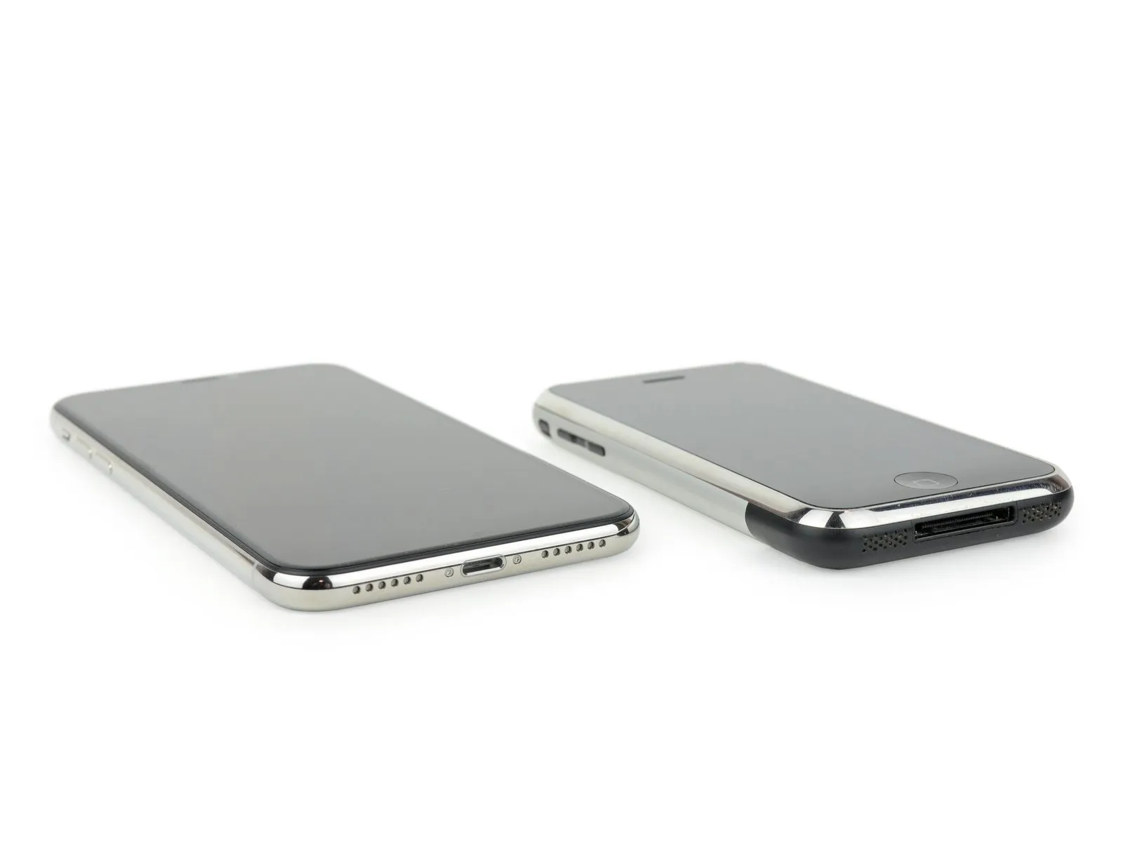
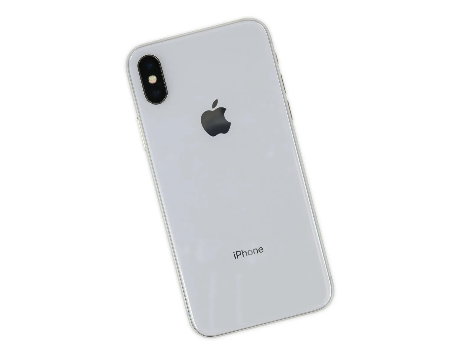
- Over a decade of iPhone evolution has resulted in a design that echoes earlier models, presenting a resemblance to the initial iPhone generation.
- However, distinguishing characteristics remain, including the prominent camera protrusion, polished stainless steel band, glass construction, and the Lightning connector...
- Consistent with the iPhone 8 released previously, Apple has eliminated the regulatory markings from the rear casing.
- The design now incorporates a seamless, smooth rear surface, aligning with a long-held design aspiration; it is hoped these devices will be properly recycled and not discarded as waste.
Step 3
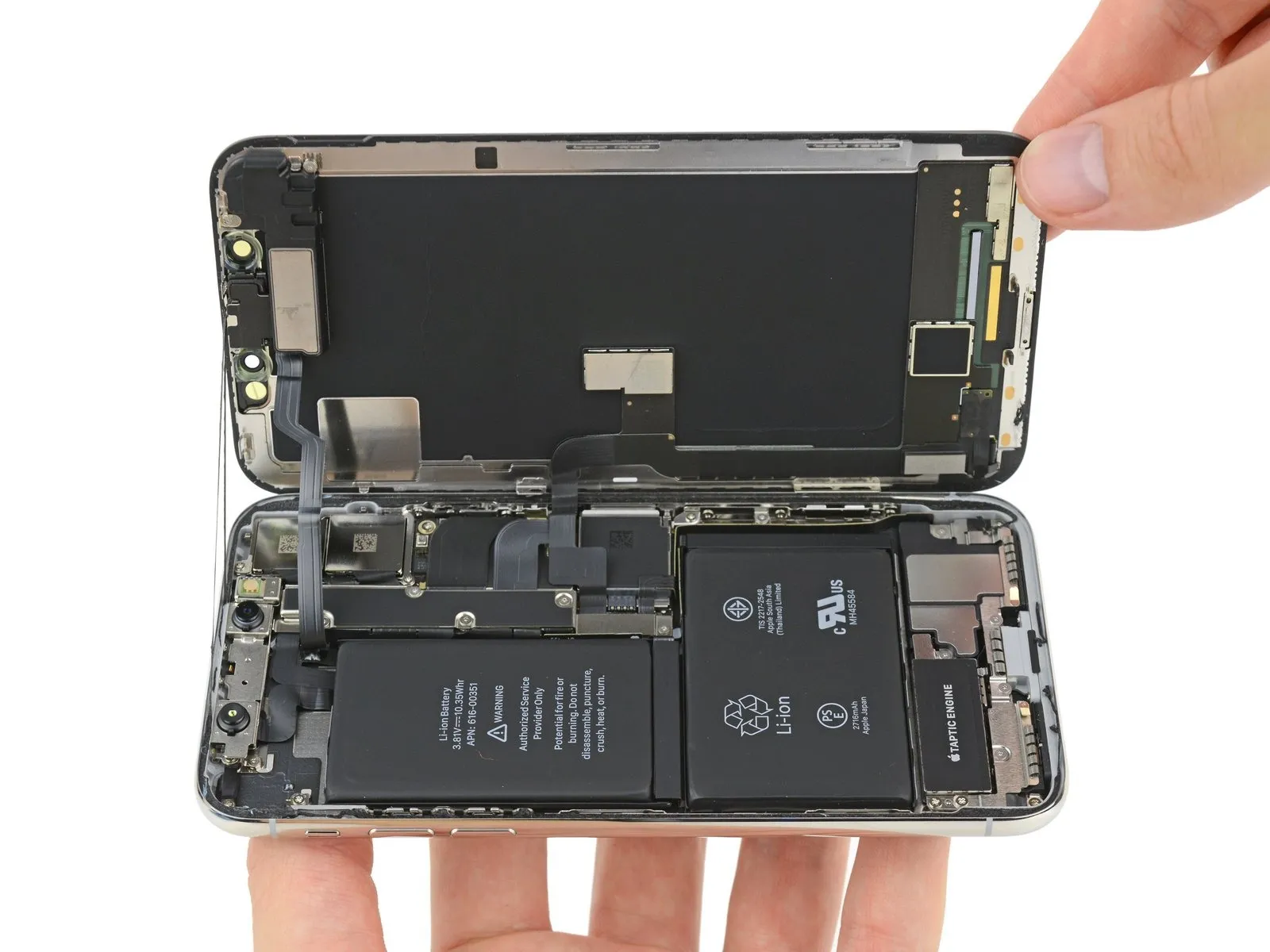
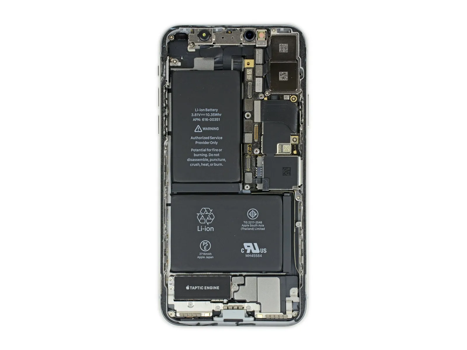
- The device incorporates a dual-cell battery configuration, a novel design feature for iPhones.
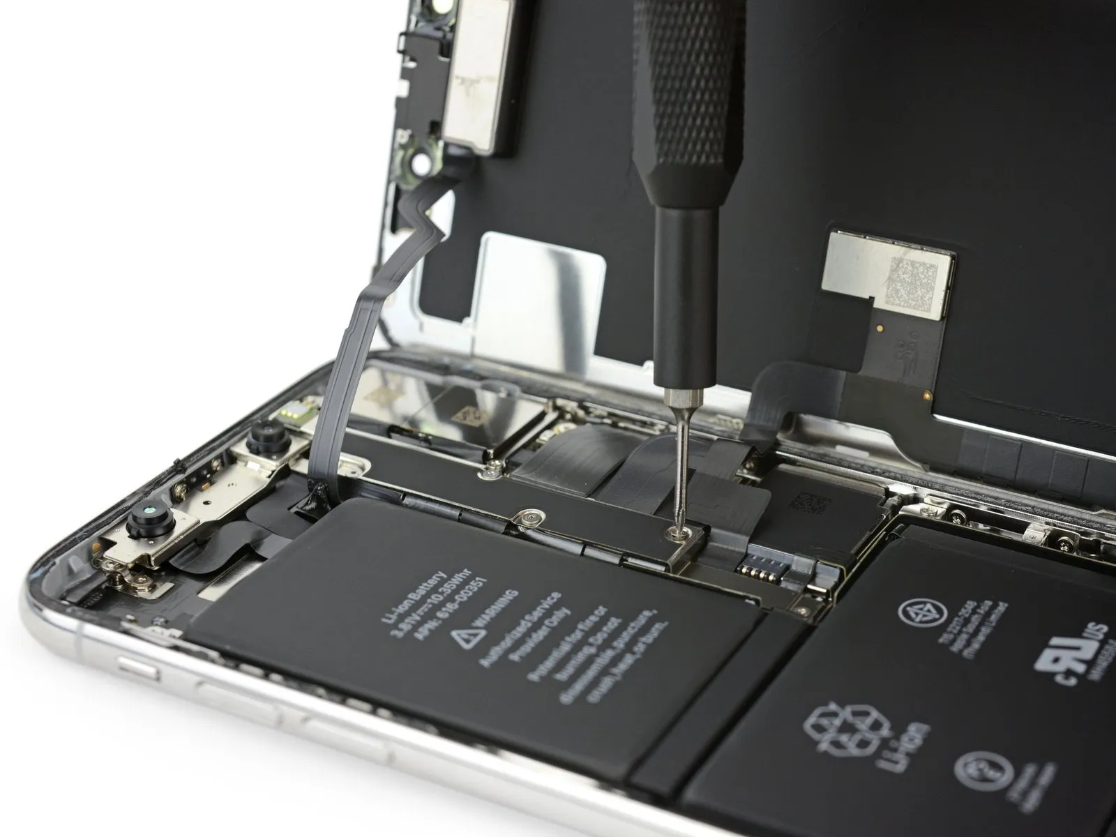
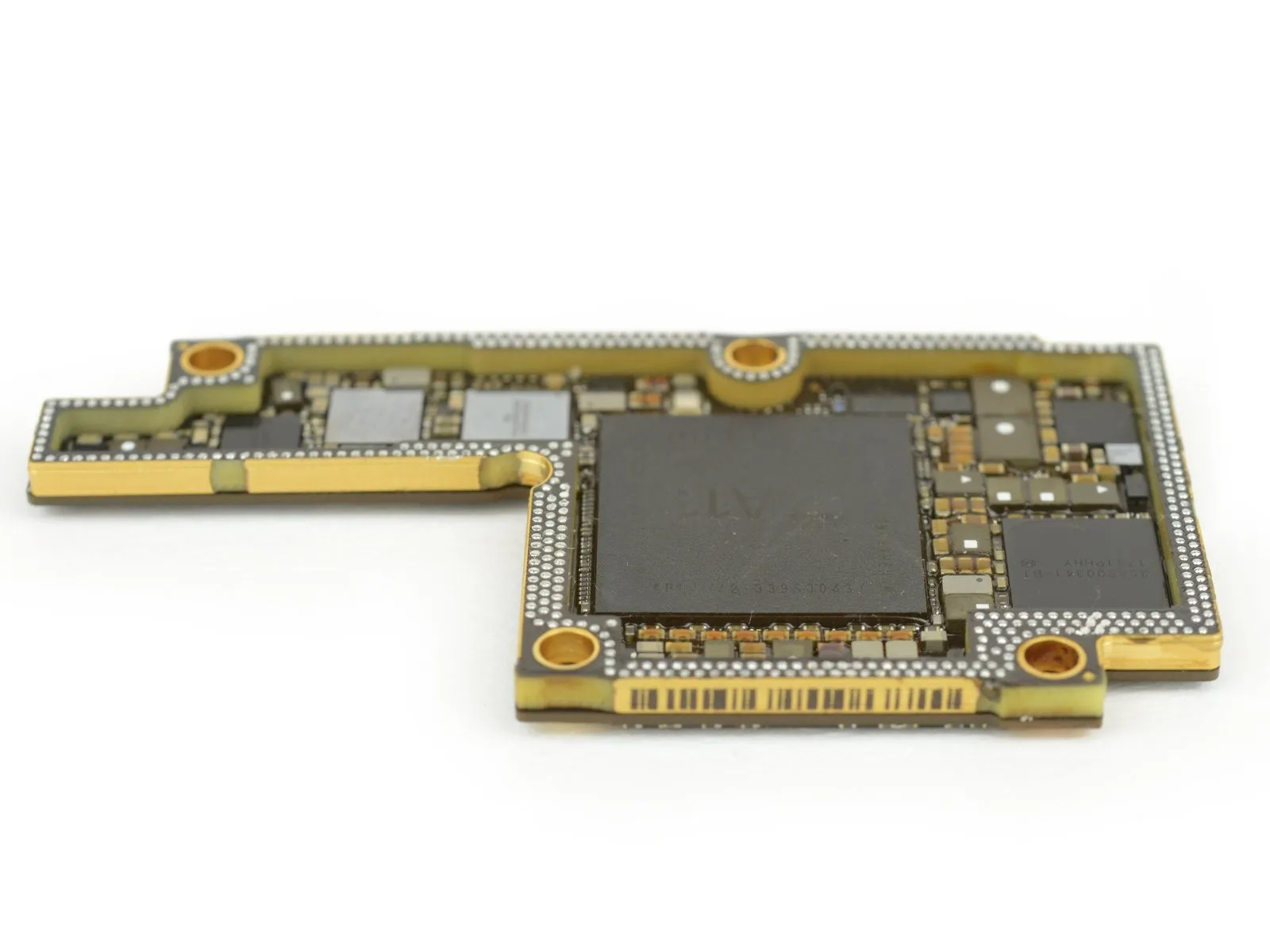
- The logic board exhibits a remarkably compact design, suggesting a two-layered stacked construction as indicated by the solder point placement.
- The earpiece speaker's position has been significantly lowered to accommodate the additional front-facing sensors.
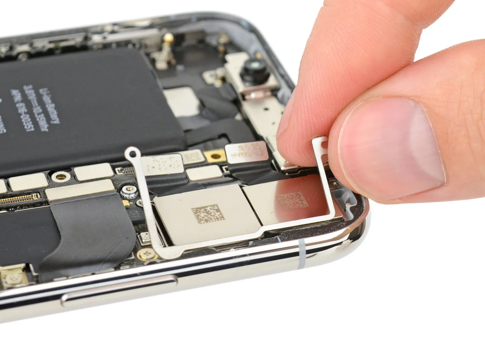
- An unidentified integrated circuit is located between the Taptic Engine and the lower speaker, prompting investigation into its function.
Step 4

- The pentalobe screw exhibits an unusual, incomplete appearance; the lower screws resemble pins rather than properly formed fasteners.
- This particular screw shifts the threaded portion from the display assembly to the steel chassis, simultaneously lengthening the non-threaded section into an exceptionally elongated pin.
- We hypothesize that this design choice provides a degree of flexibility for the display panel, while also enabling the repositioning of its mounting bracket closer to the phone's internal components, which incidentally creates space for a more robust Lightning connector.
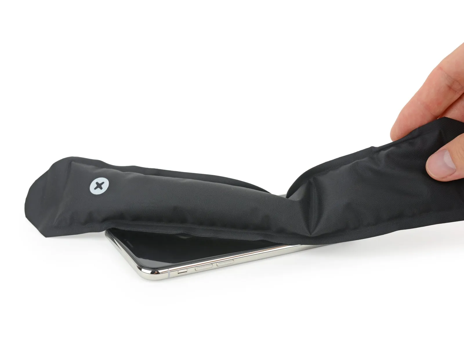
- Fortunately, the internal layout appears largely unchanged, as the standard tools—an iOpener, an iSclack, and iFixit Opening Picks—function effectively as they previously did.
- Consequently, the resistance encountered remains consistent, and the OLED panel is adequately supported by a surrounding frame, a feature absent in certain other displays.
Step 5
- The design featuring a side-facing screen has become a consistent feature of iPhones, initially introduced by Apple with the 7 Plus and now a commonplace characteristic.
- This particular enclosure encompasses all logic board connections, representing an unprecedented level of connector concentration.
- As is typical, tri-point screws are positioned to obstruct repairs beyond the initial pentalobe screws securing the device's casing.
- It appears Apple intends to discourage user intervention and internal modifications.
Step 6
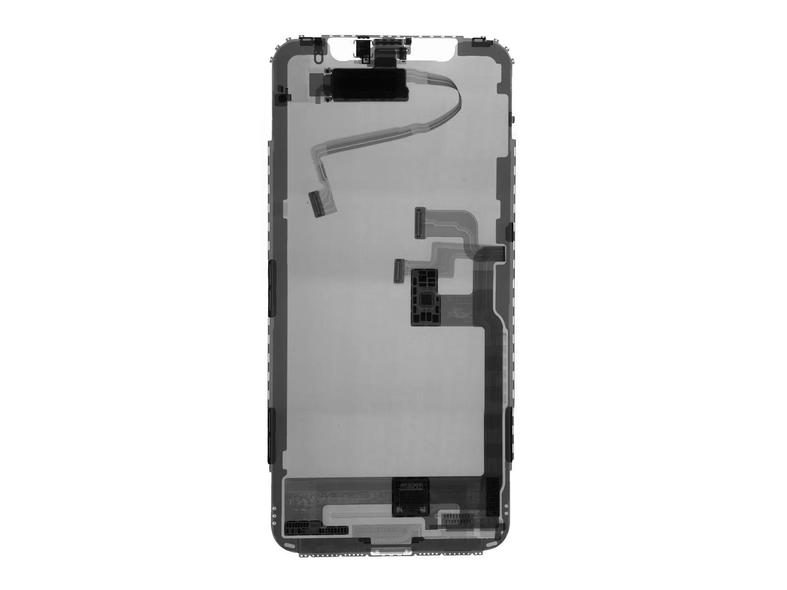
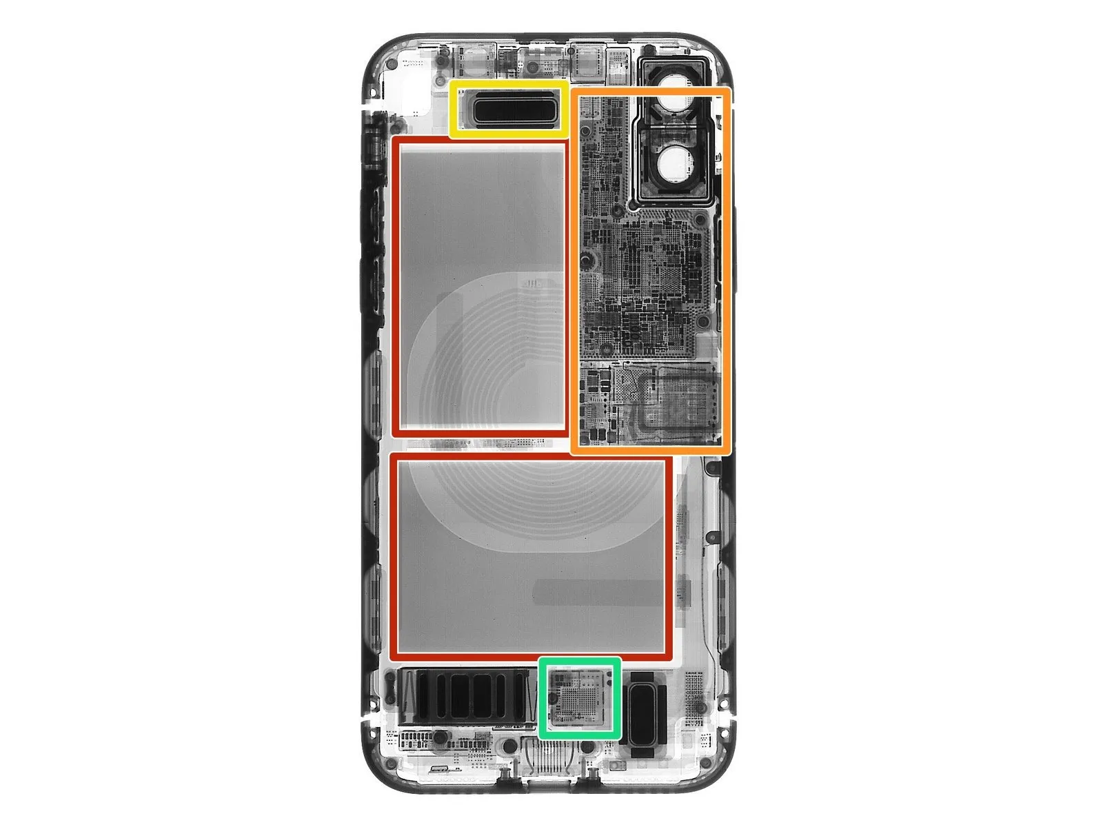
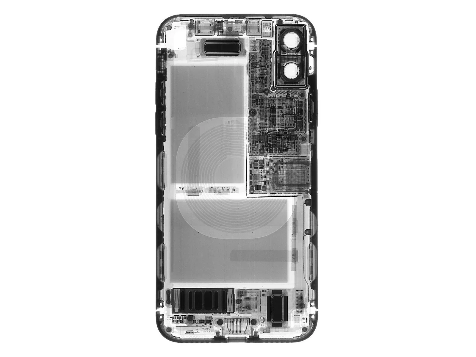
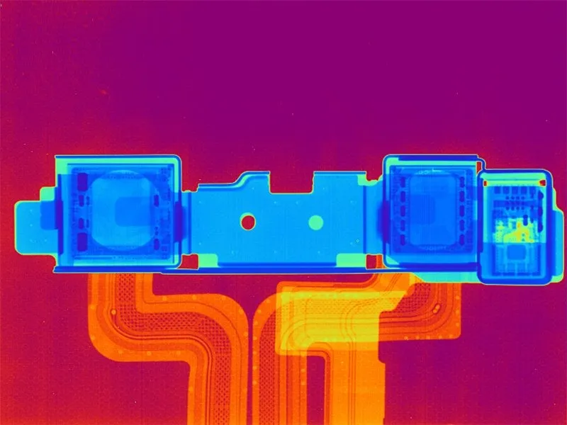
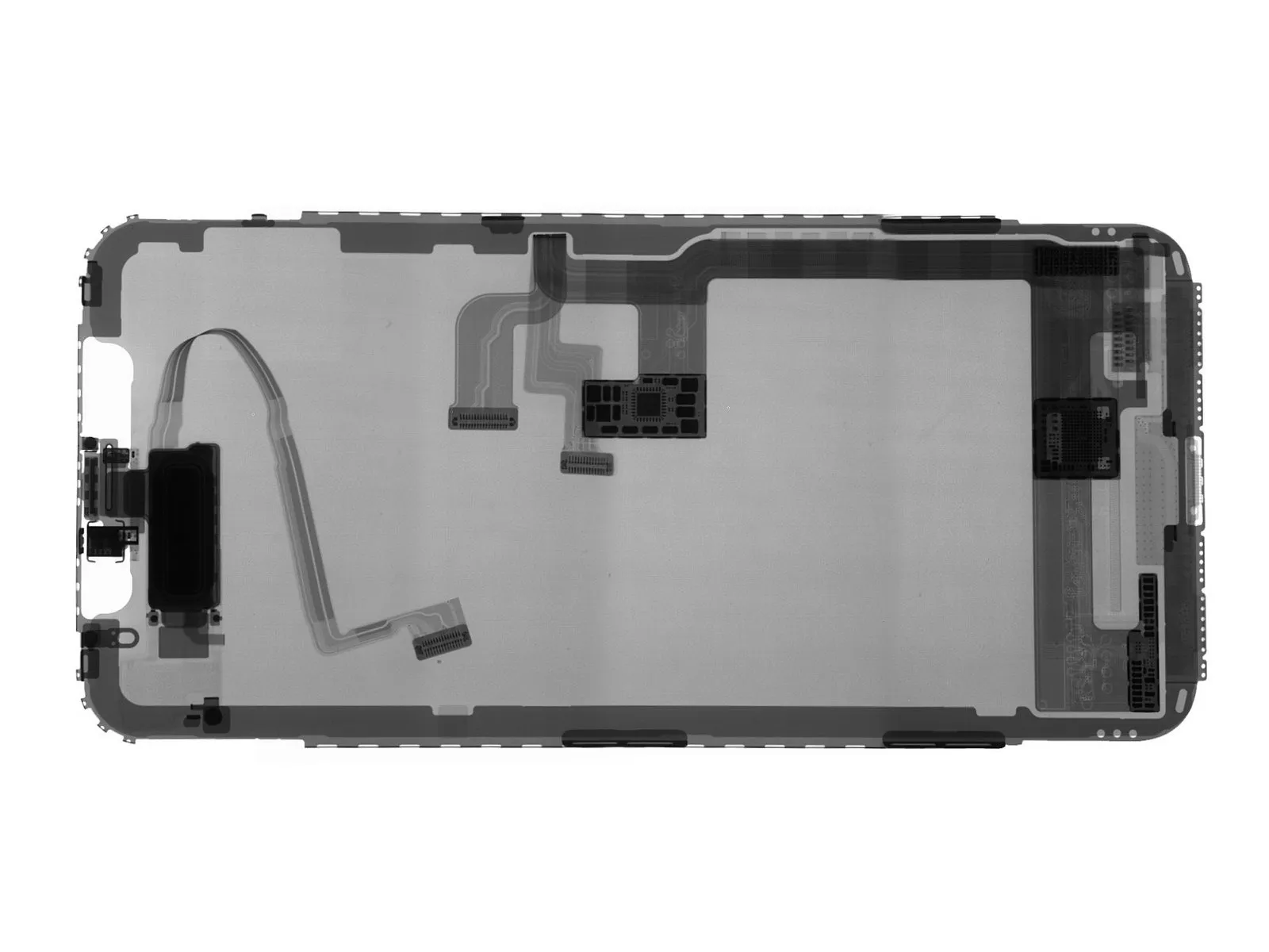
A more detailed examination of the hardware affixed to the screen will follow presently; at this juncture, we confirm through X-ray imaging that the unidentified integrated circuit is attached to the display panel.
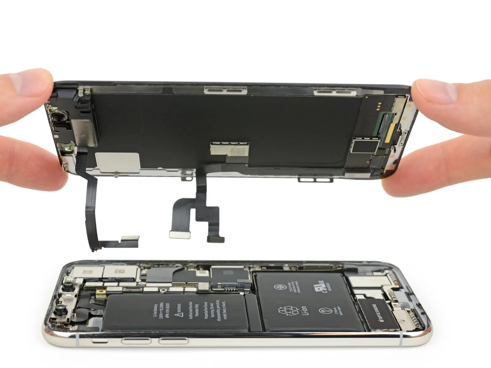
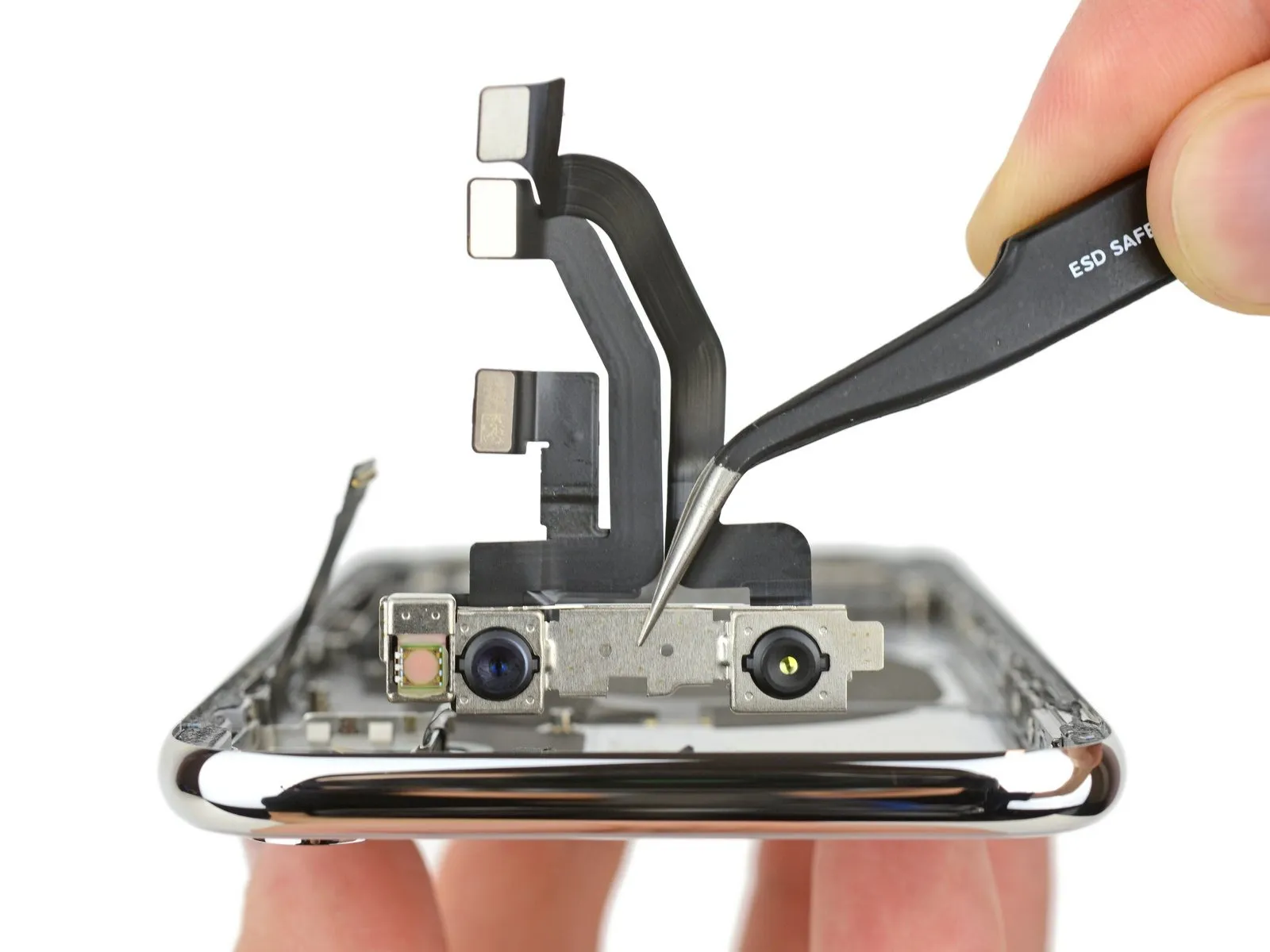
As a departure from the previous steps, the display assembly detaches, leaving the front-facing camera in place.
This comprehensive visual inspection validates the arrangement previously identified via X-ray analysis: the majority of the internal volume is dedicated to the innovative dual-cell battery, and the logic board’s physical dimensions have been considerably reduced.
Step 7
Foam adhesive further secures the camera modules to the rear enclosure, preventing unwanted movement and ensuring stability. Maintaining the cameras' fixed position is essential for the proper functionality of Portrait Mode and related image processing features.
Minute spot welds are visible around the perimeter of the camera housing cover glass, likely serving to firmly attach the camera bump structure to the device's chassis.
Step 8
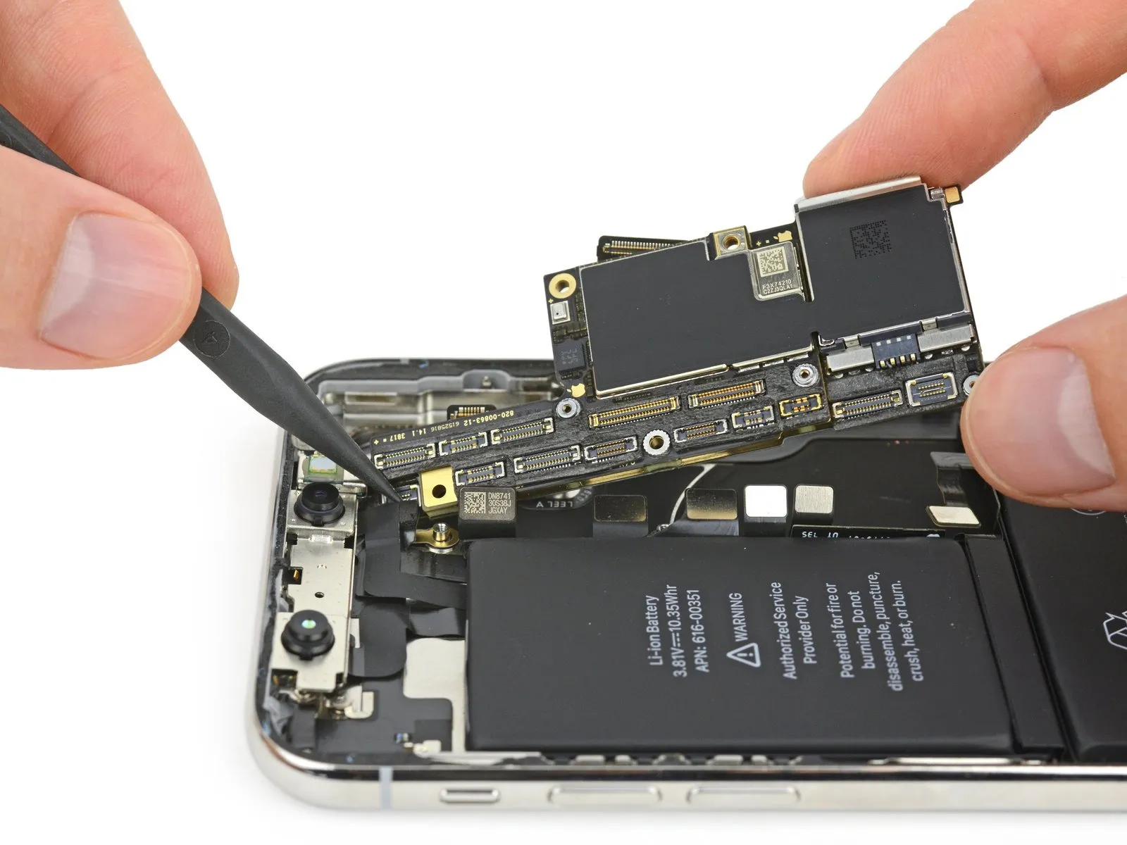
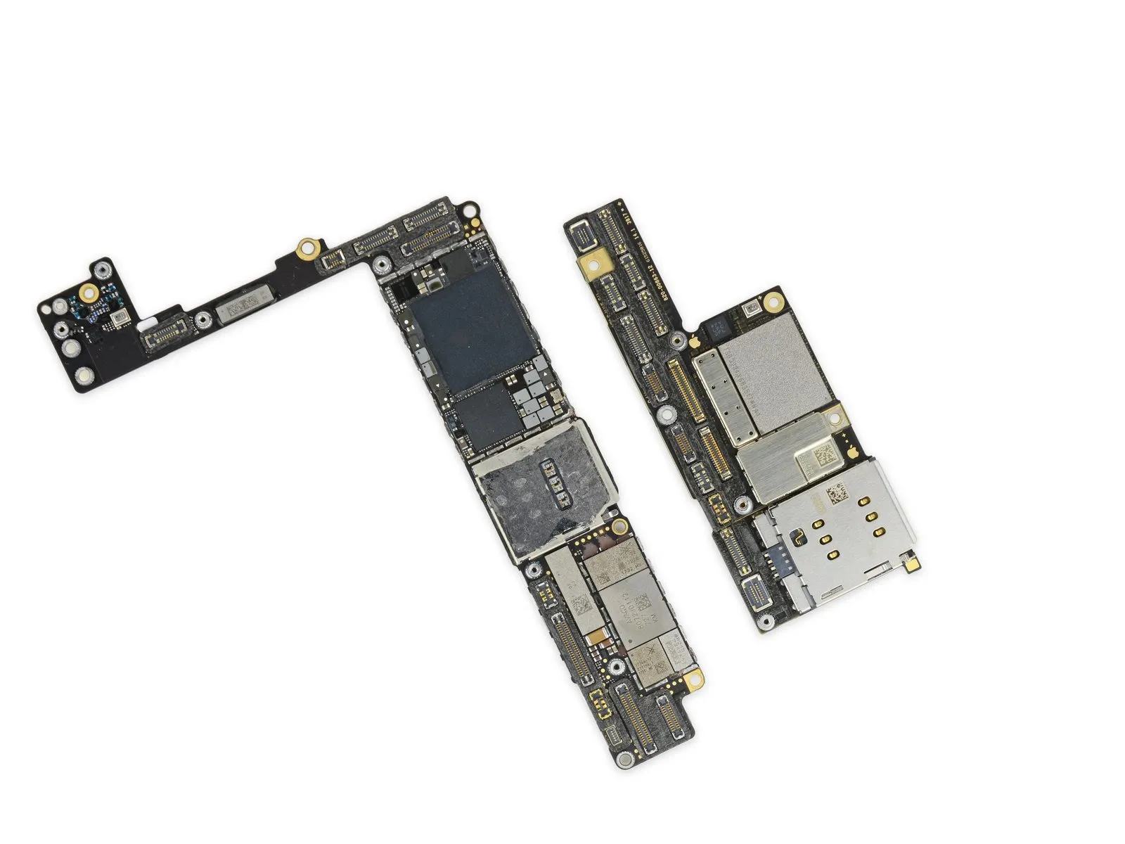
Due to its diminutive size, this logic board exhibits exceptional space utilization; the concentration of connectors and components represents a significant advancement in miniaturization, surpassing even the component density found in an Apple Watch by weight.
The iPhone X's remarkably small circuit board accommodates a greater quantity of electronic components, creating a stark contrast in size and layout when positioned alongside the iPhone 8 Plus's larger board.
An analysis of the physical dimensions reveals that the iPhone X motherboard occupies approximately 70% of the area covered by the iPhone 8 Plus motherboard, resulting in a considerably larger area available for the battery.
Step 9
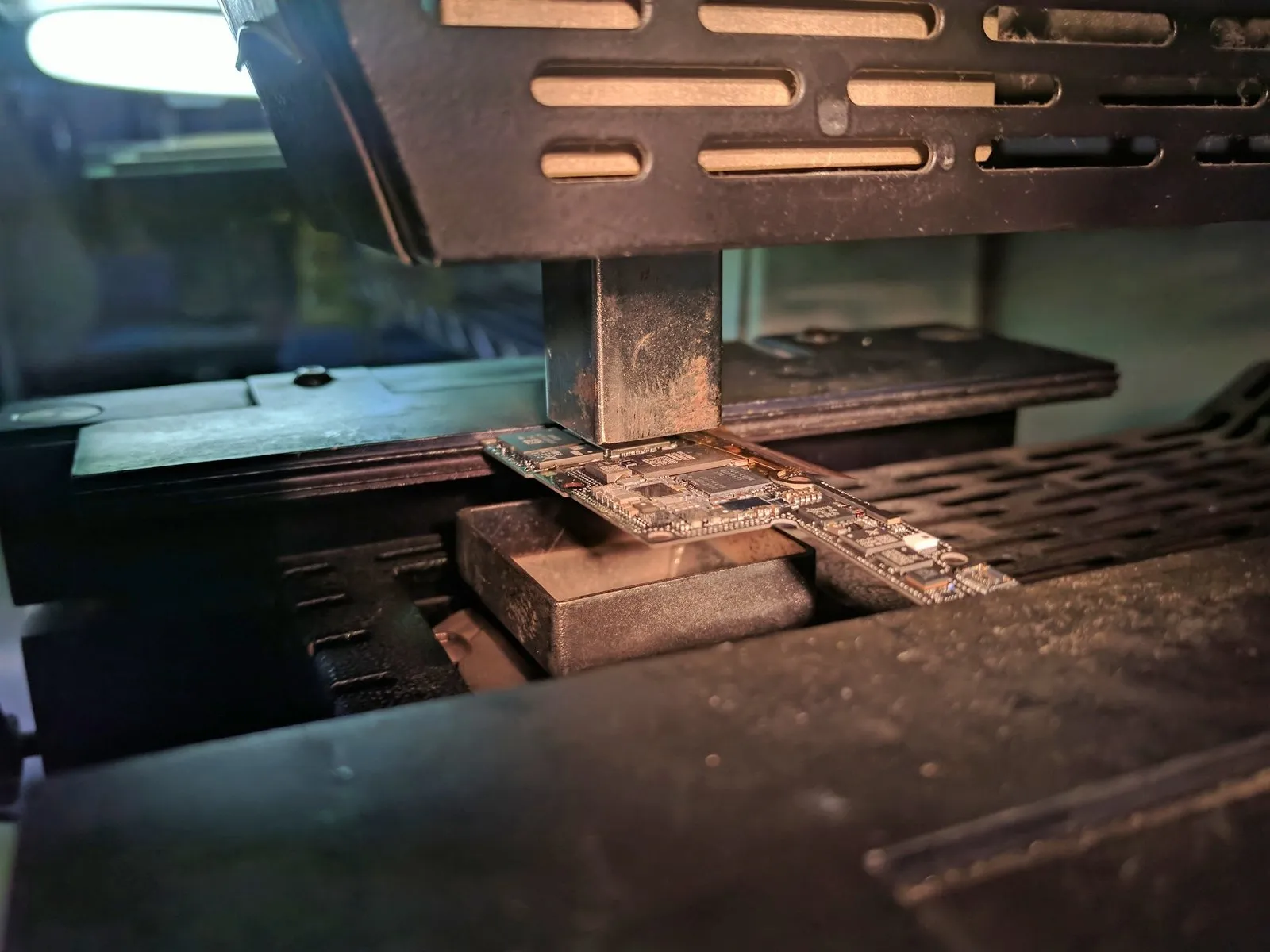
- Due to the layers being joined by solder, we enlisted the assistance of Circuitwise and utilized their BGA hot air rework equipment to carefully delaminate the board's sections.
- Following the separation of the components, a measurement of each layer's surface area was performed, revealing a combined total of 135% of the logic board area found in the iPhone 8 Plus – a testament to Apple’s efficiency in maximizing component density.
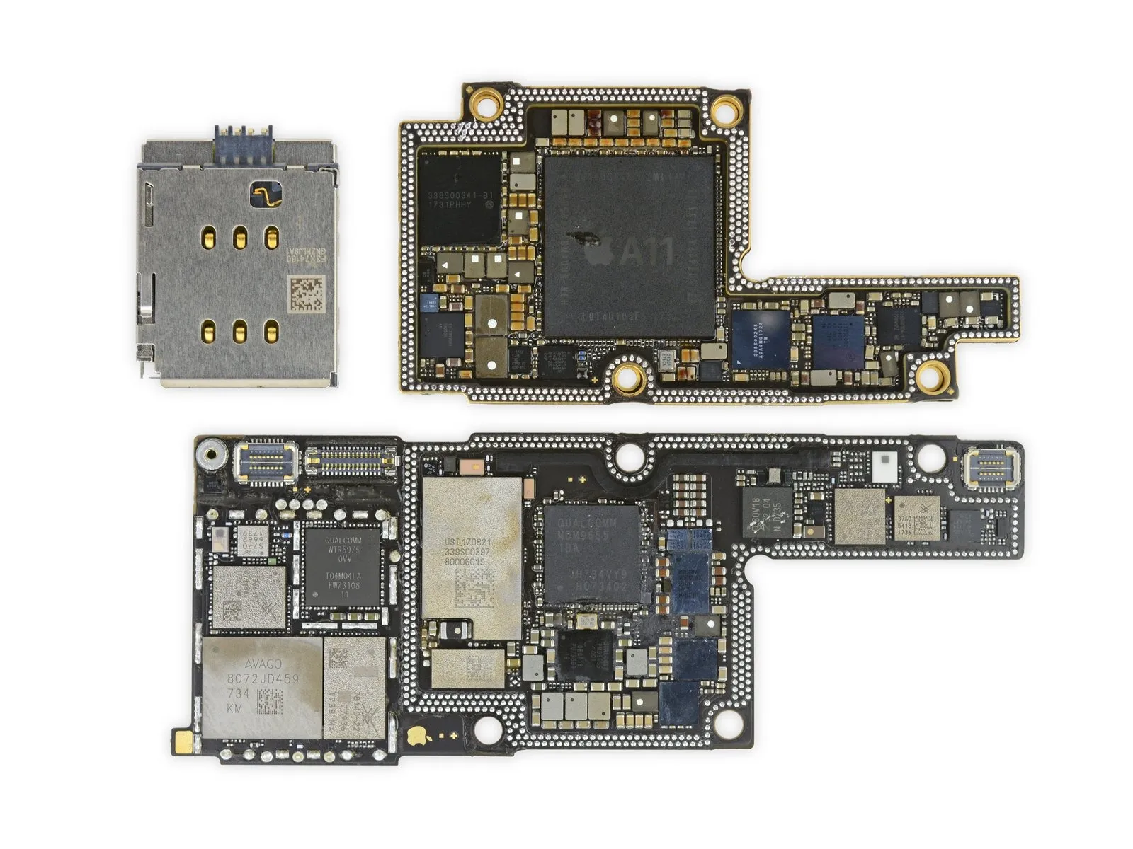
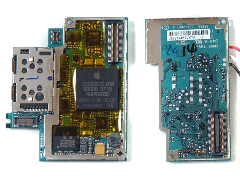
- The logic board within the iPhone X represents the initial instance of a double-stacked board architecture observed in an iPhone model since the original iPhone, as depicted in the third photograph.
- However, this innovative structural approach introduces a significant challenge: board-level repairs will likely be considerably more complex.
Step 10
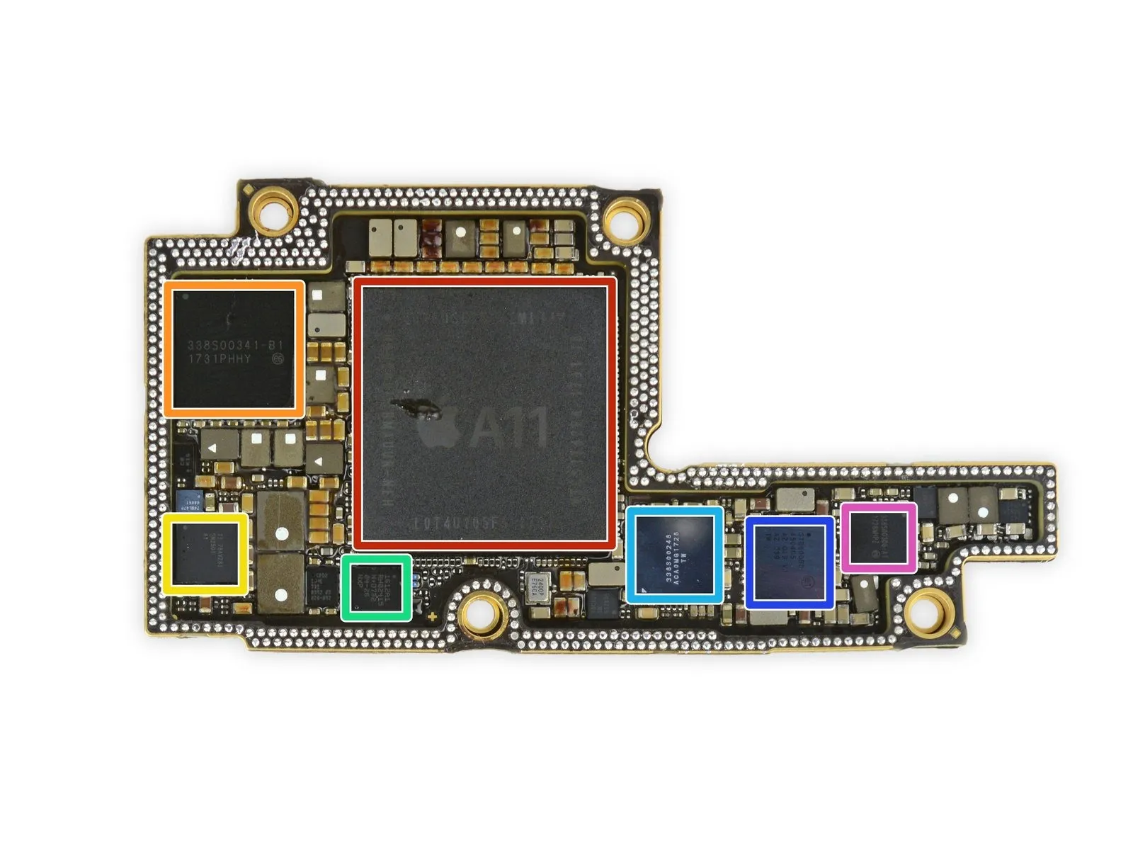
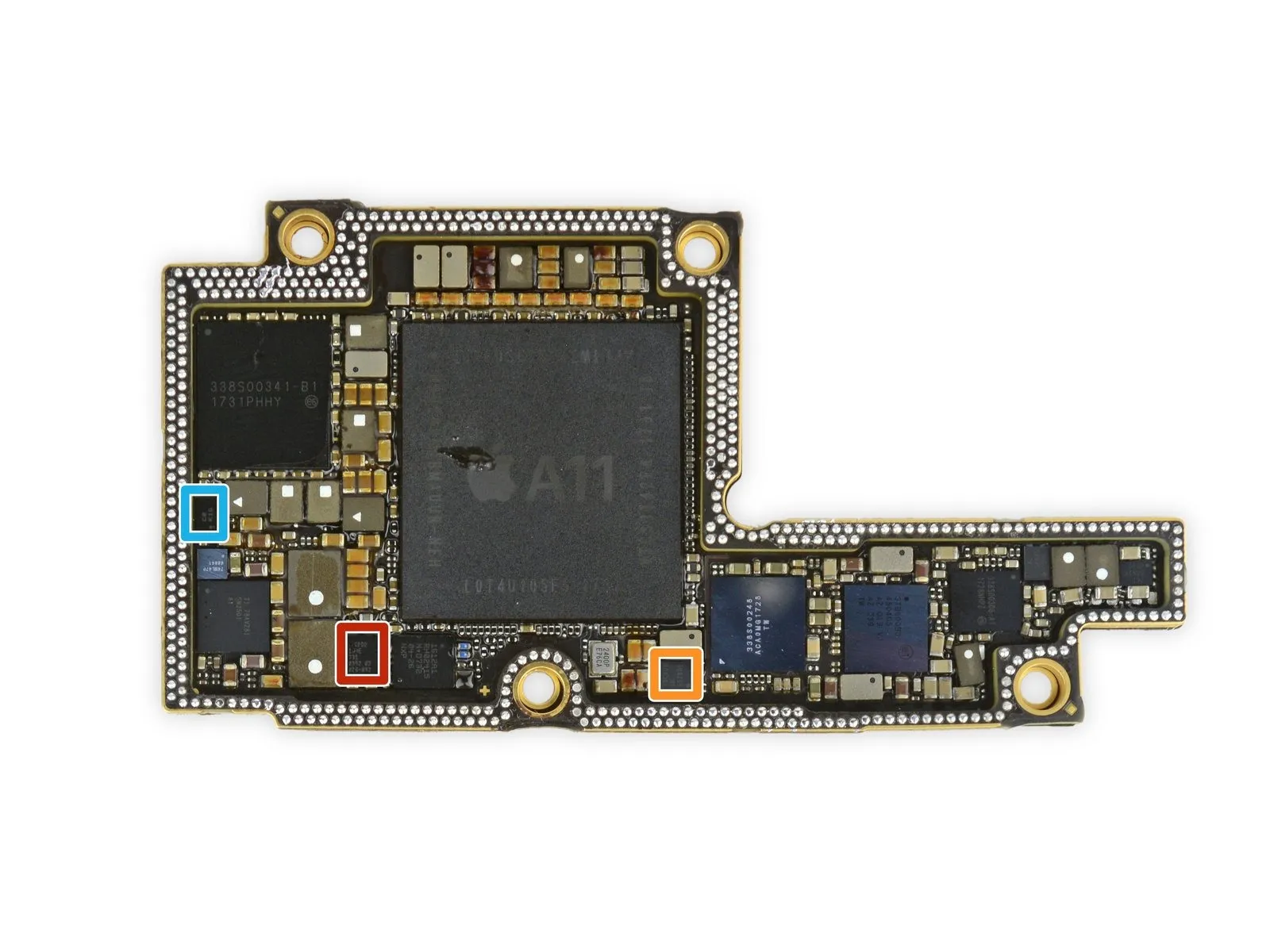
- Apple APL1W72 integrates an A11 Bionic SoC,
- built atop 3 GB of SK hynix H9HKNNNDBMAUUR LPDDR4X RAM,
- along with an Apple 338S00341-B1 power management integrated circuit,
- incorporating a Texas Instruments SN2501 battery charging unit,
- utilizing an NXP Semiconductor CBTL1612A1—probably a variation of the 1610 tristar IC,
- featuring an Apple 338S00248 audio codec,
- including STMicroelectronics STB600B0 power management,
- and also an Apple 338S00306 power management integrated circuit
Step 11
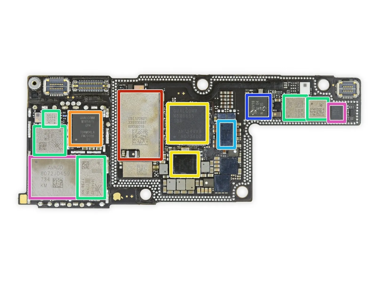
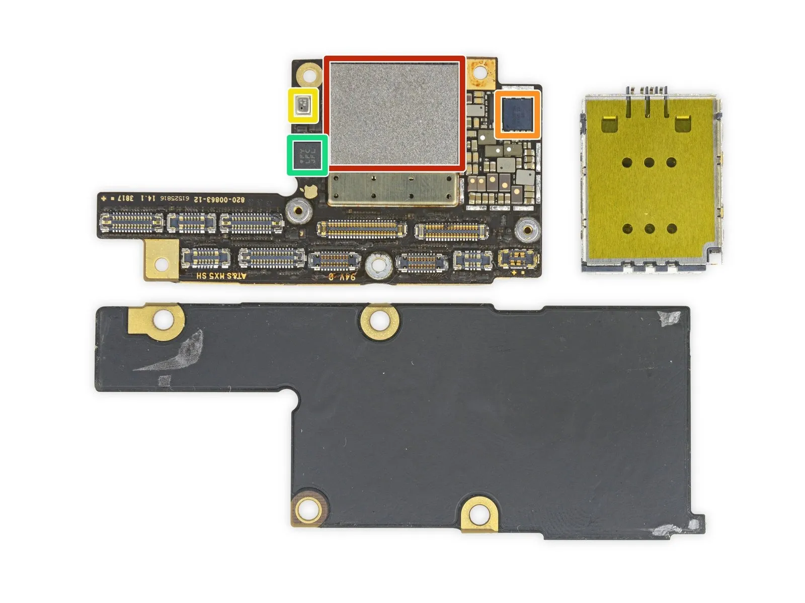
- The component identified as Apple/Murata USI 170821This device is a 339S00397 WiFi/Bluetooth module.
- A Qualcomm WTR5975 gigabit LTE transceiver is present.
- The system incorporates a Qualcomm MDM9655 Snapdragon X16 LTE modem, along with the PMD9655 PMIC; however, Apple utilizes a dual-sourcing strategy for the modem, with TechInsights’ analysis of the A1901 model revealing an Intel XMM7480 (PMB9948) component. Although the modem possesses the capability, Apple has chosen not to enable gigabit speeds using the Qualcomm component.
- The device includes a Skyworks SKY78140-22 power amplifier, a SKY77366-17 power amplifier, along with the components S770 6662, 3760 5418, and 1736.
- A Broadcom BCM59355 serves as the wireless charging controller.
- The NFC functionality is managed by an NXP 80V18 PN80V controller module.
- An AFEM-8072 and MMMB power amplifier module are also included.
Step 12
Externally, affixed to the logic board assembly, you'll find:
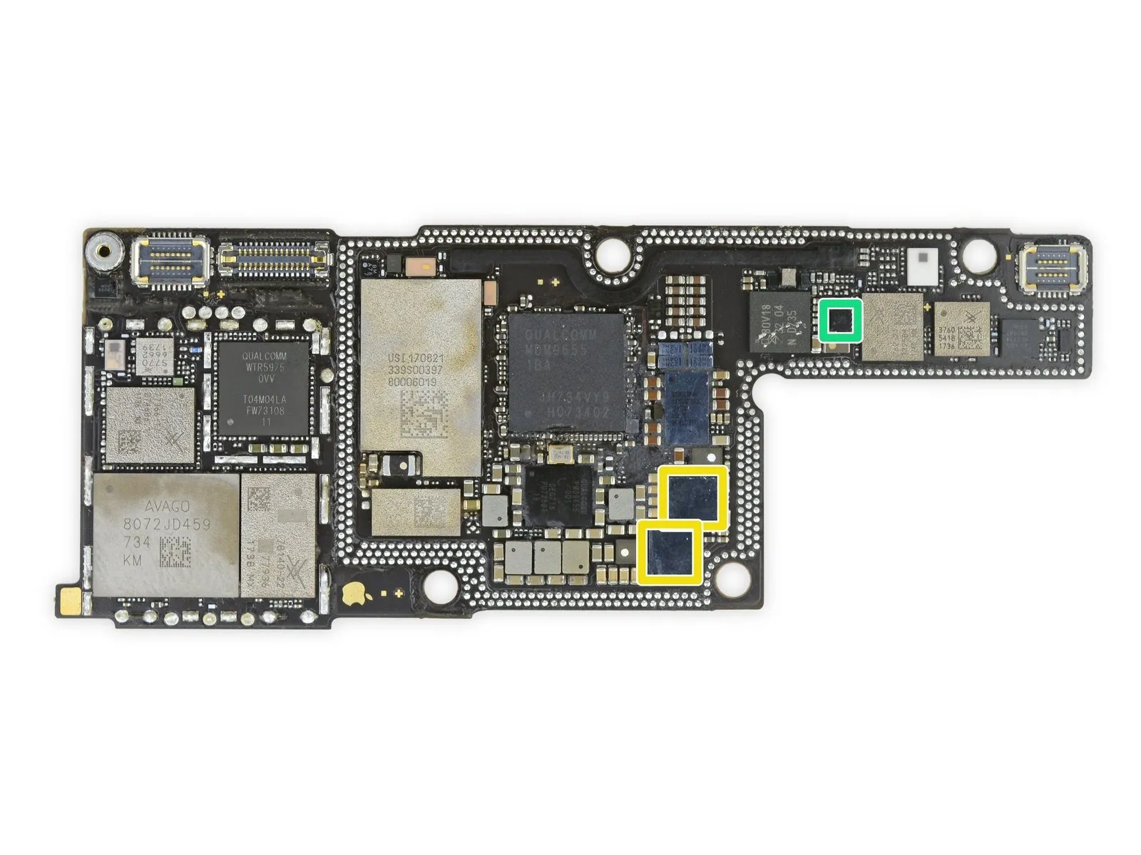
- A Toshiba TSB3234X68354TWNA1 component is present.The device incorporates 64 GB of flash memory.
- An Apple/Cirrus Logic 338S00296 audio amplifier is also mounted.
- A Bosch Sensortec BMP282 pressure sensor is integrated into the design.
- A Bosch Sensortec gyroscope and accelerometer combination is included.
Step 13
Further identification of integrated circuits:
- A Cypress Semiconductor component,is designated as CYPD2104,and functions as a USB type-C port controller.
- A Texas Instruments device,model SN61280E,serves as a Li-ion DC-DC converter.
- An Apple/Cirrus Logic component,identified by part number 338S00296,provides audio amplification.
- An ON Semiconductor component,performs the role of a DC-DC converter.
- A SiTime MEMS oscillator is also present.
Step 14
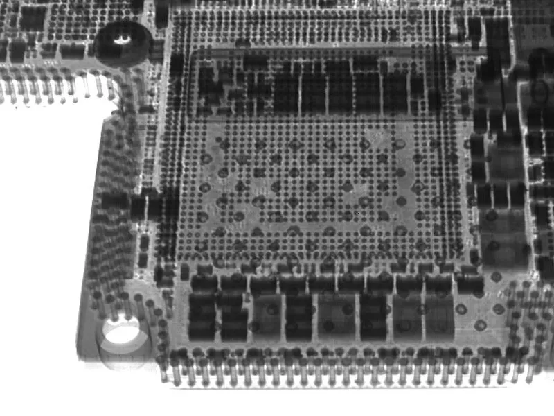
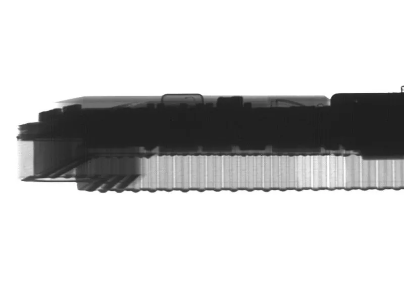
Let's examine how Apple's layered printed circuit board (PCB) assembly functions.
To achieve this design, a secondary spacer PCB was fabricated, precisely aligning along the edges. Rather than utilizing a delicate flexible cable for interconnection, data transmission occurs through numerous through-hole vias.
Within this construction, theA11 SoC is situated centrally on the primary board. Visualizing the board's three-dimensional arrangement is possible through examination of the X-ray images. The cylindrical features observed around the periphery represent openings filled with solder, establishing electrical connections between the two board layers.
Step 15
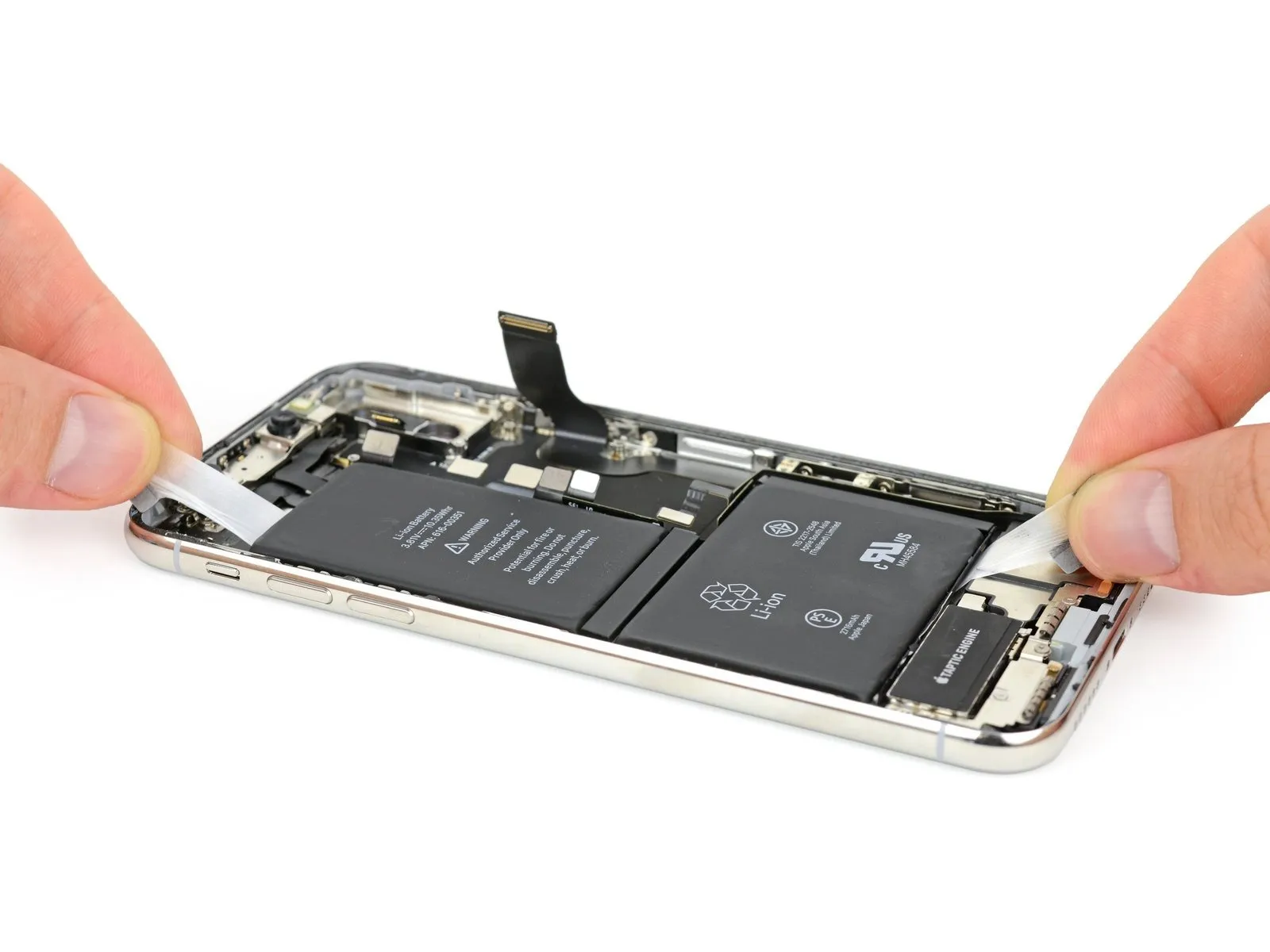
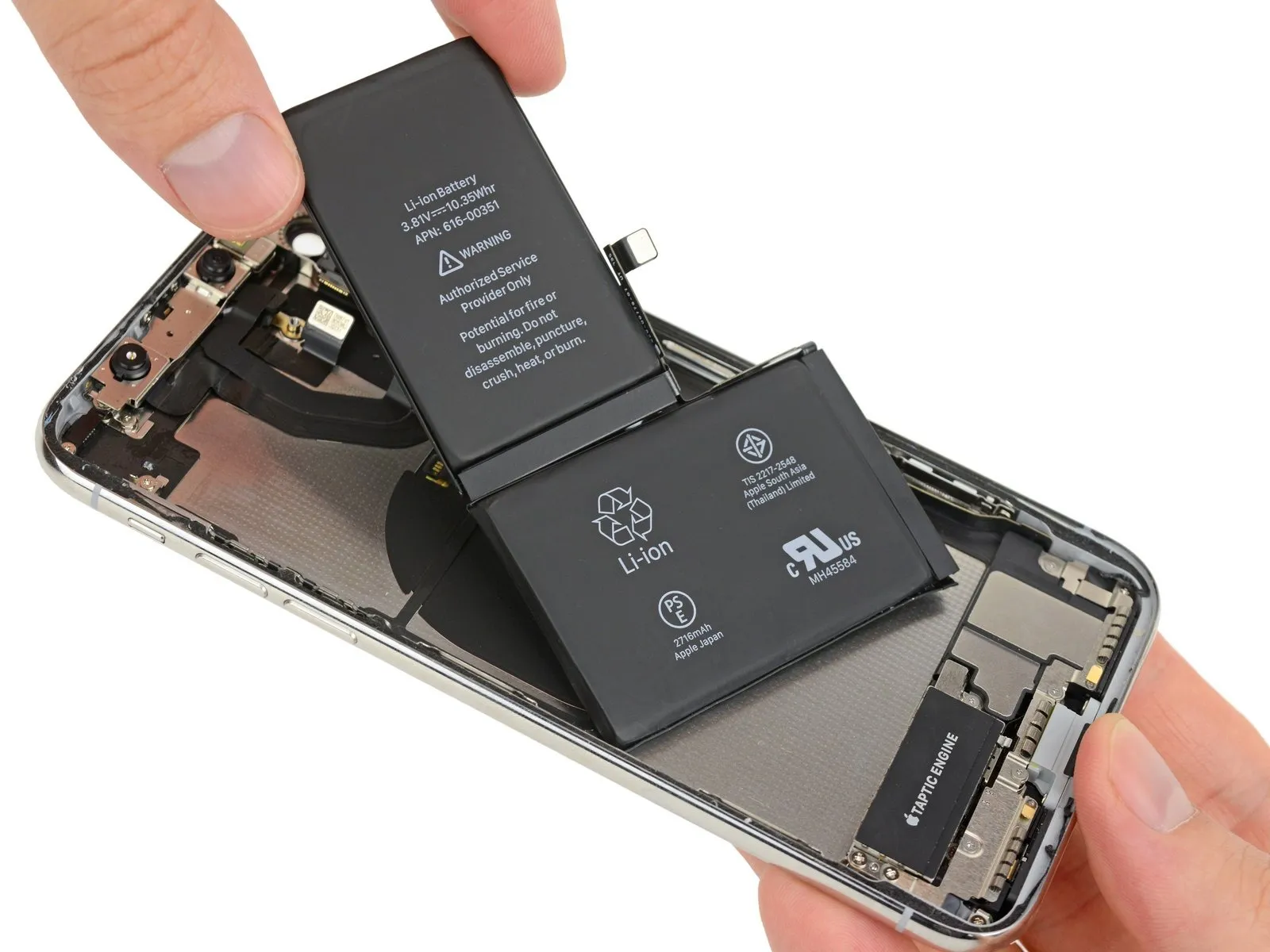
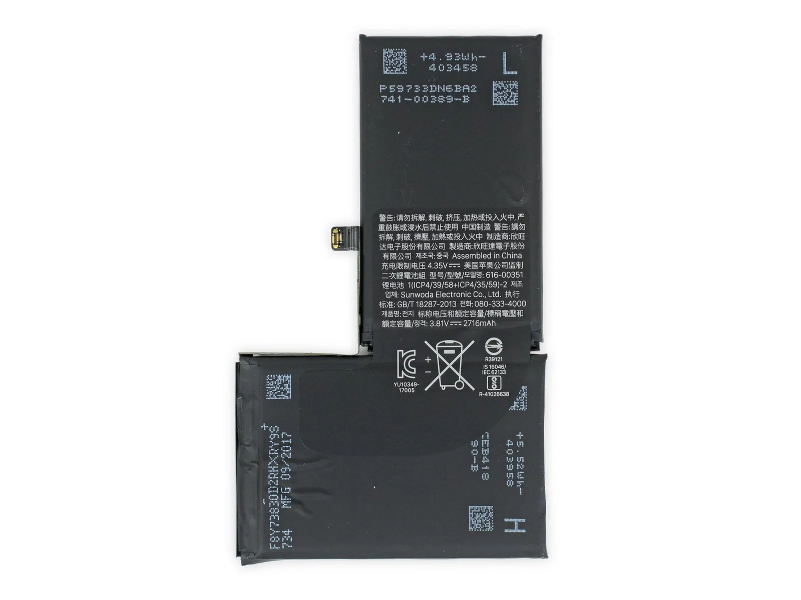
Resembling the shorter pull-tabs previously observed in the 8 series, the newly installed dual-celled battery incorporates four such tabs, but positioned in a completely different arrangement.
Unlike previous designs where tabs were folded over the top, these are affixed to the sides of the battery cells, which introduces a slightly more complex repair process.
Inside this device, you'll discover a 10.35 Wh energy capacity, equivalent to 2716 mAh at a voltage of 3.81 V, marginally surpassing the 10.28 Wh capacity of the 8 Plus battery– although it remains less powerful than the Galaxy Note8's 12.71 Wh large-scale battery.
The adoption of a dual-cell configuration primarily serves to optimize internal space, rather than significantly increase overall capacity; it enables more flexible shapes and positioning to effectively utilize the available room resulting from the logic board's reduced size.
Step 16

- Let's delve into some background:Previously, Microsoft developed a sophisticated spatial sensor known as the Kinect.
- The infrared dot matrix technology that drove this sensor originated from the Israeli technology firm,PrimeSense.
- Apple acquired PrimeSense for a substantial $360 million in 2013, and has undoubtedly committed hundreds of millions more to its refinement and commercialization.
- Consequently, Microsoft was compelled to create a replacement sensing system for the Kinect 2; it's conceivable that the iPhone's inclusion of a depth sensor may lead to its integration with drones.
Step 17
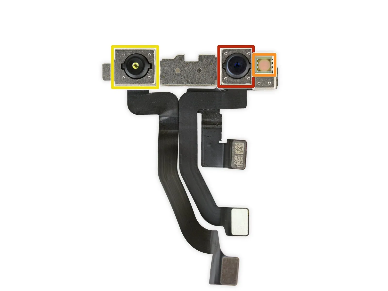
- An infrared (IR) light source, integrated within the display, illuminates your face.
- The front-facing camera, identifiable by its red marking, verifies the existence of a face.
- Positioned on the far right, the IR dot projector casts a pattern of dots across your face, generating a three-dimensional representation.
- The IR camera, situated on the left side, captures this dot pattern and transmits the resulting data to the device's processor.
- Internally, the X utilizes advanced software algorithms to process the sensor data and determine identity, distinguishing between yourself and a potential duplicate.
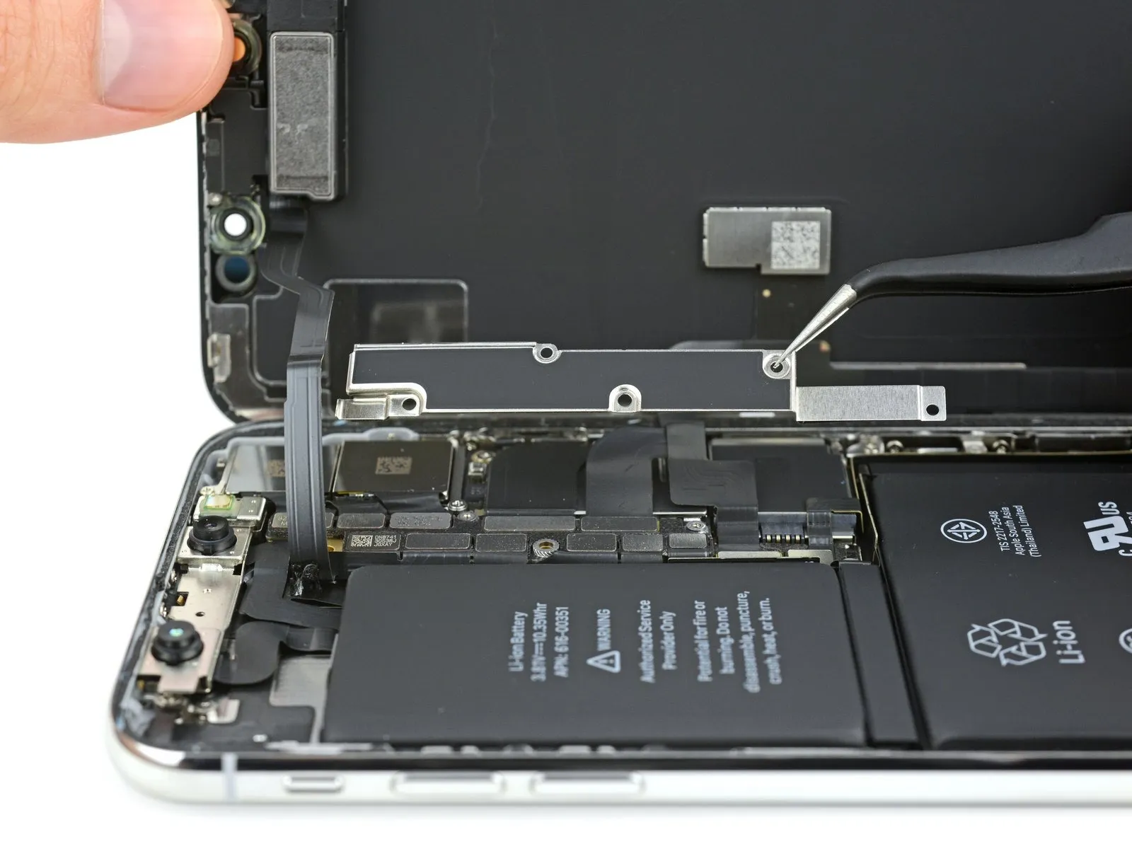
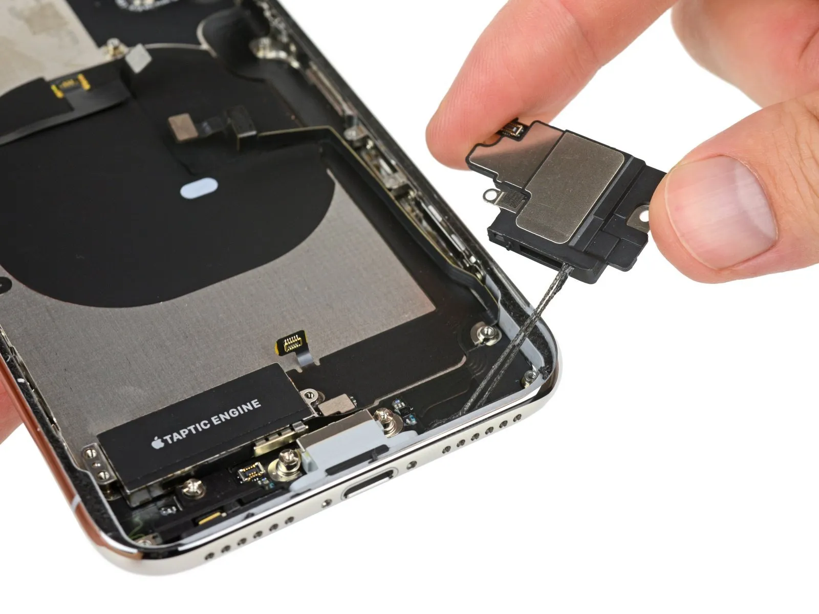
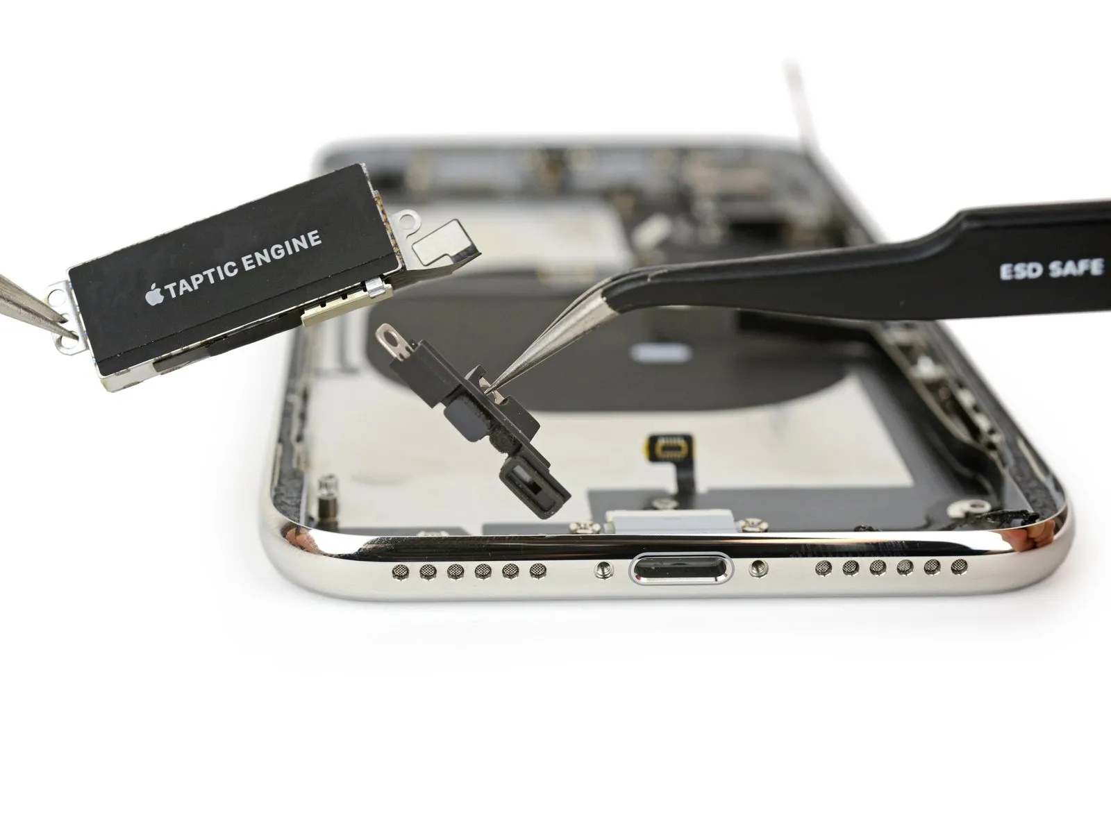
Step 18
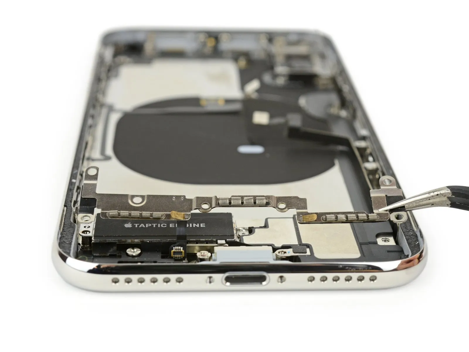
- The initial bracket to be removed features spring connectors, EMI grounding contacts, and a ribbon cable adhered to its reverse side.
- Following this, the lower speaker enclosure is extracted, exhibiting a substantial amount of waterproofing adhesive surrounding the port.
- Finally, the Taptic Engine and the well-known barometric vent are detached; Apple's Taptic Engine remains a linear oscillating vibration motor.
Step 19
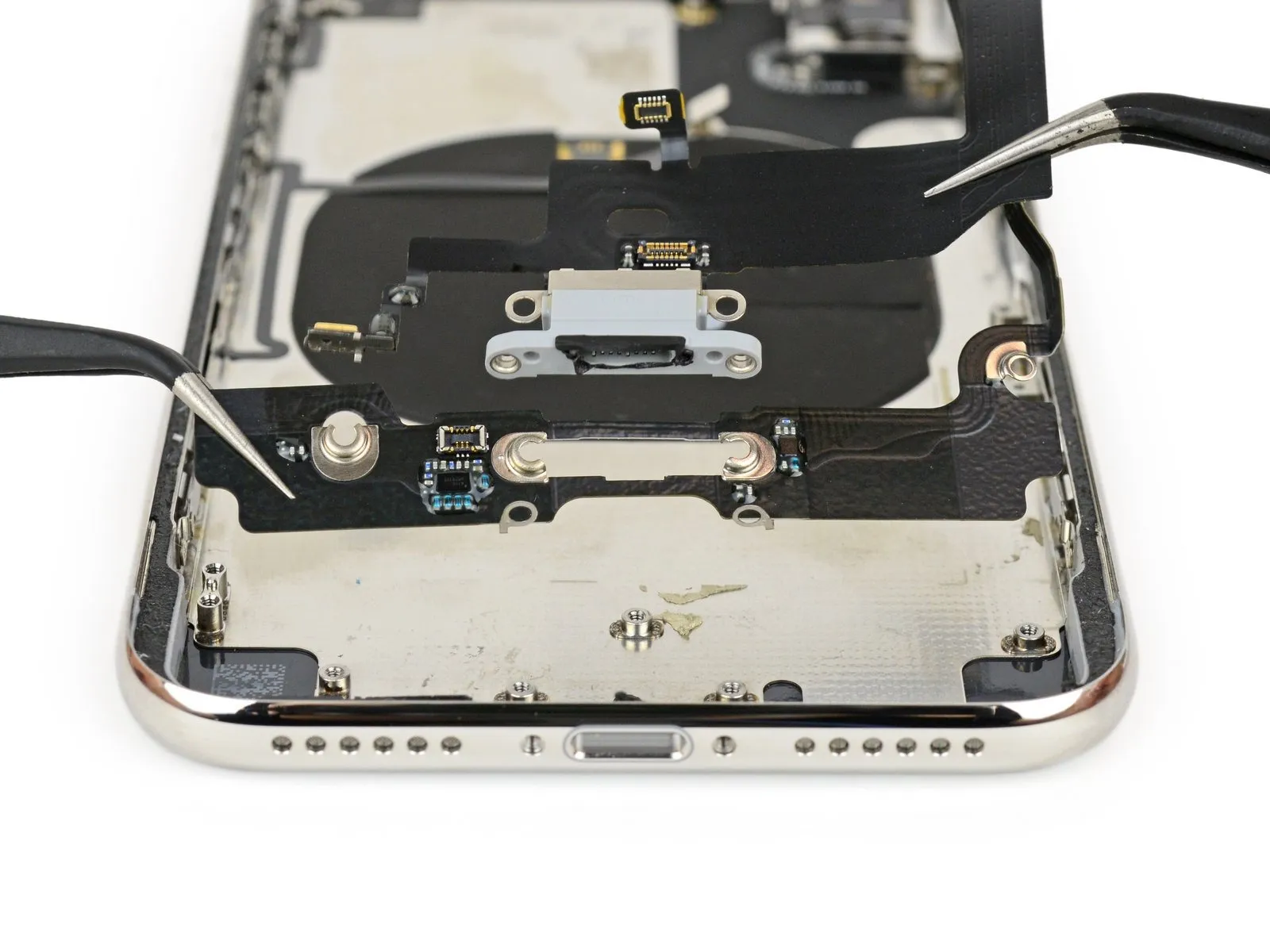
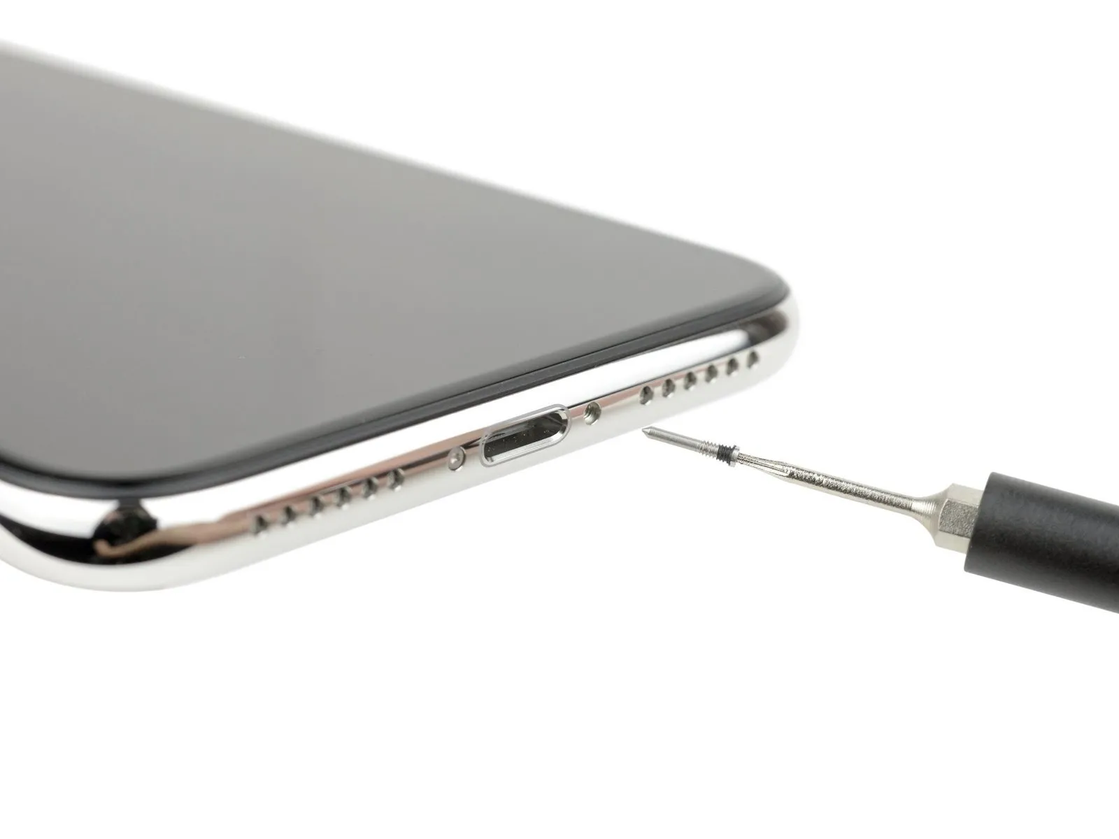
- Those experiencing issues with a loose or unstable charging cable will be pleased to observe that the Lightning connector exhibits enhanced durability, incorporating a broadened mounting bracket secured to the frame's side with screws.
- Furthermore, the design includes openings allowing the exterior pentalobe screws to extend and engage with the display, mirroring a previously observed detail.
Step 20
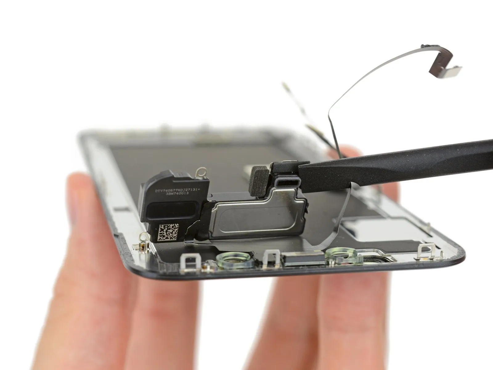
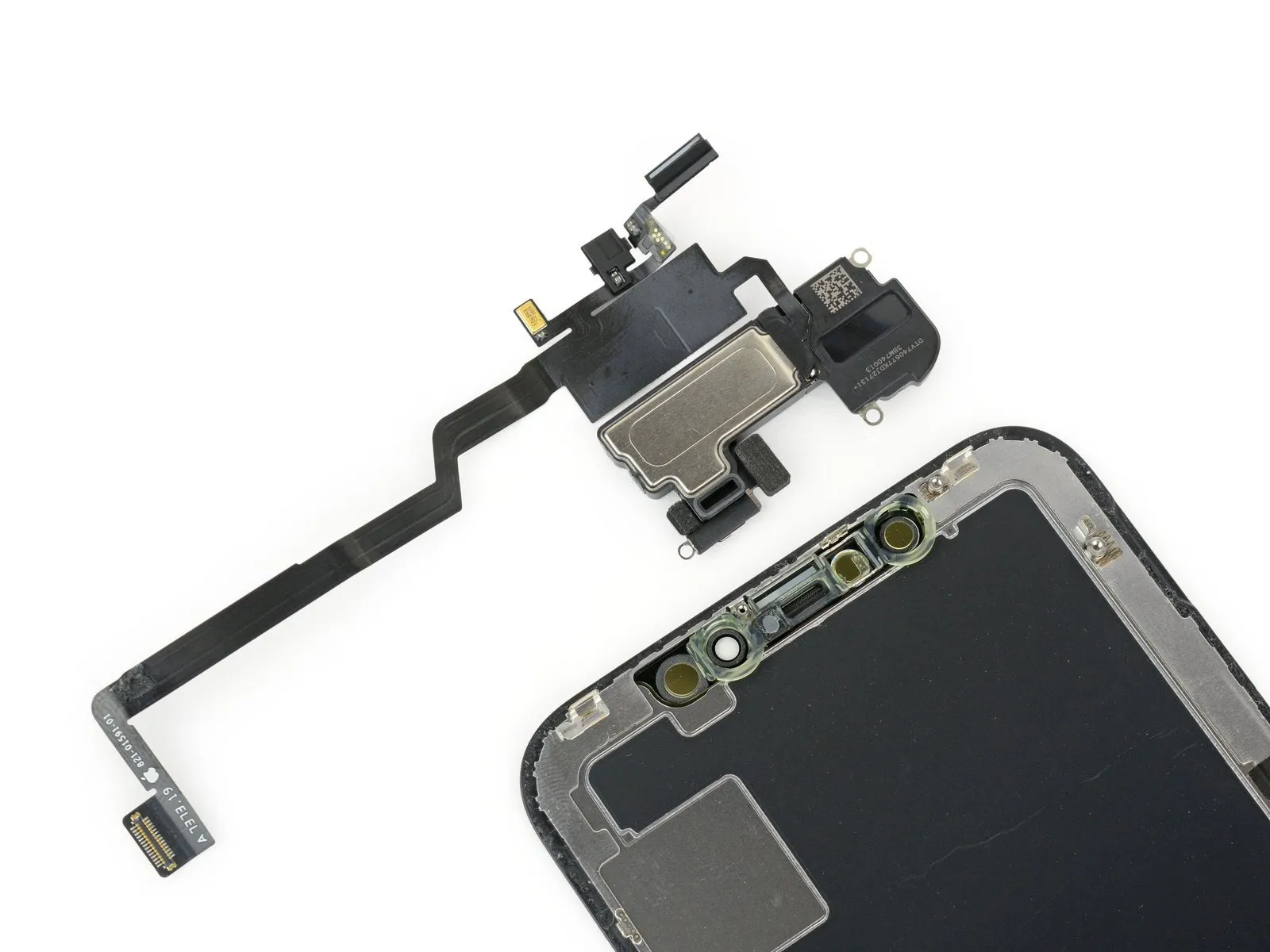
- Immediately noticeable is the earpiece speaker, which features a novel duct designed to direct audio output from the display.
- Detailed removal of the upper display components reveals a particularly intricate assembly of components, including a loudspeaker, microphone, ambient light sensor, flood illuminator, and proximity sensor.
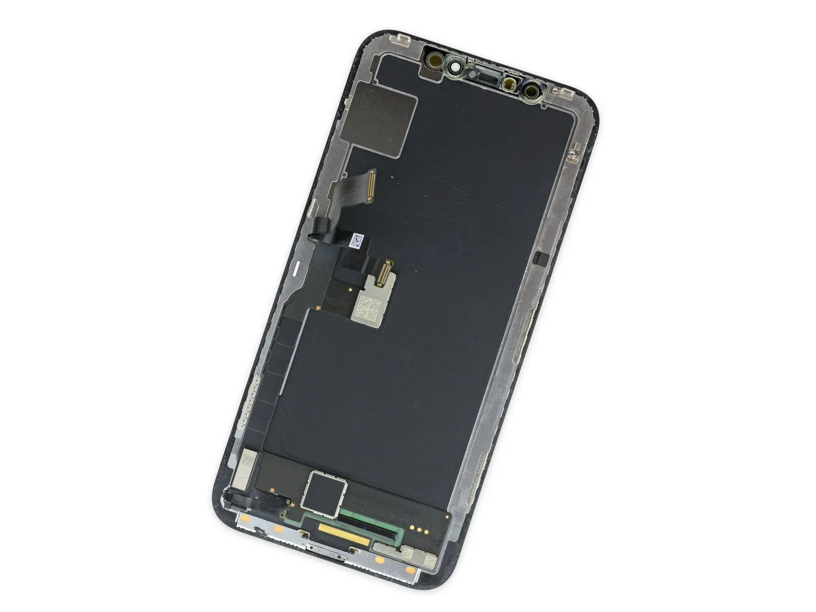
- Once all of the detachable modules are removed, only the bare display remains.
Step 21
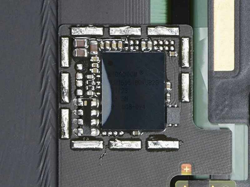
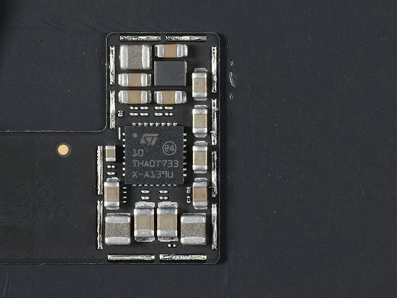
- A Broadcom touchscreen controller, identified as BCM15951B0KUB2G.
- Accompanying this component is a previously unobserved STMicro device, which is an OLED power management integrated circuit designated 10 THADT733 X-139U.
Step 22
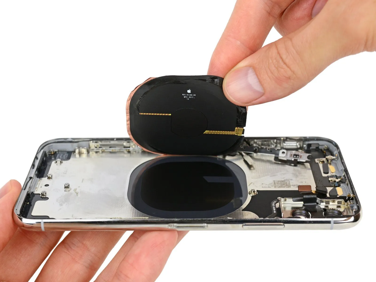
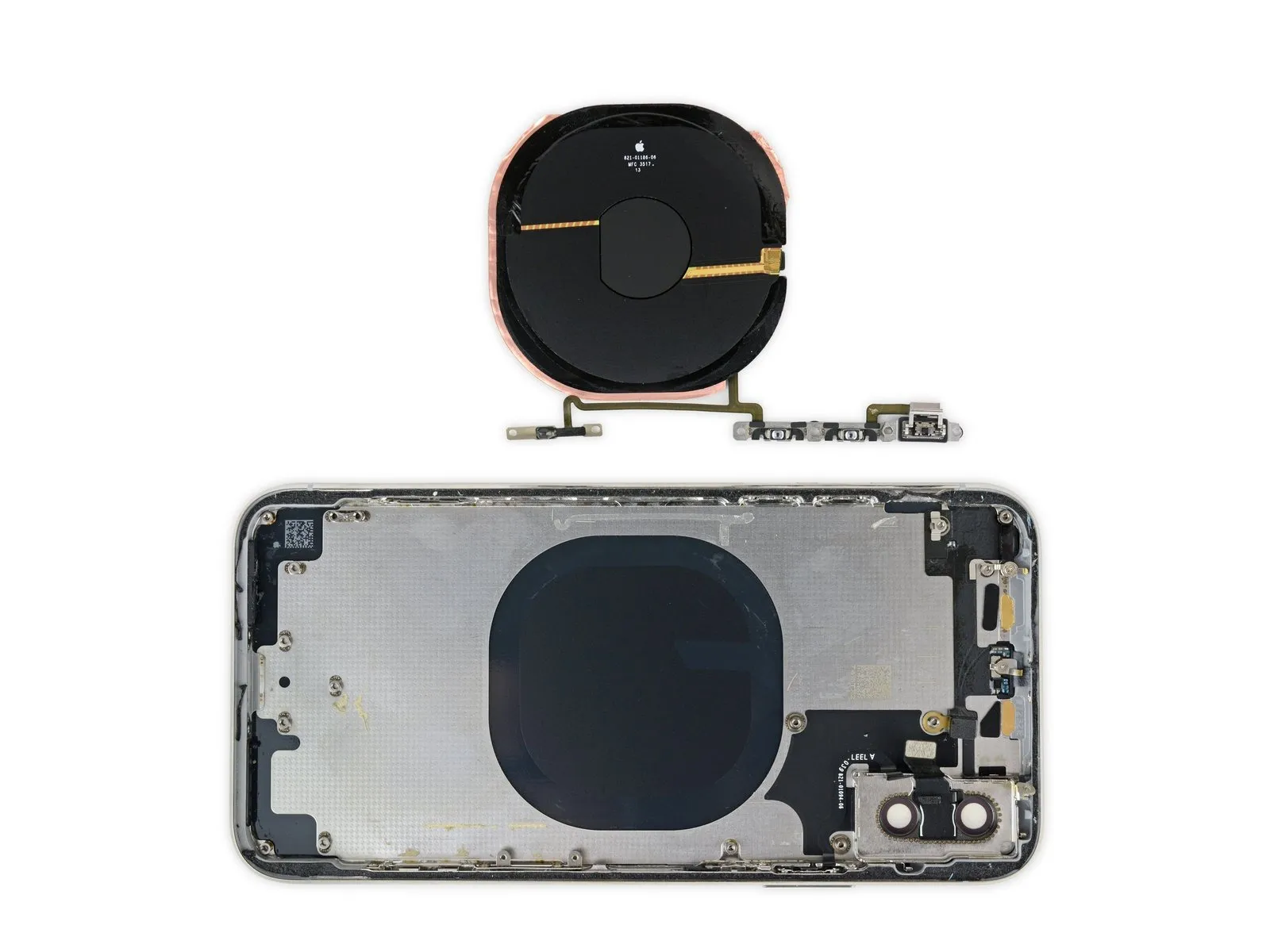
- Upon reaching the bare metal chassis, a recurring component within this intricate design emerges: the wireless charging coil.
- Notably, all components affixed to the coil must be considered, encompassing the volume buttons, the ring/silent switch, and an unidentifiable sensor bracket.
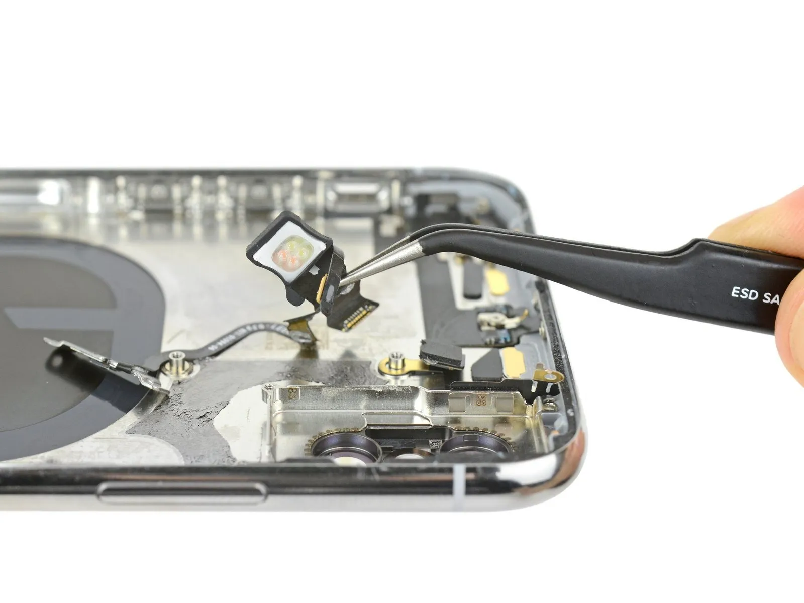
- Furthermore, the complex multi-function cable located at the phone's apex is carefully extracted; this unit incorporates the quad-LED True Tone flash and the power button, mirroring designs found in earlier iPhone models.
Step 23
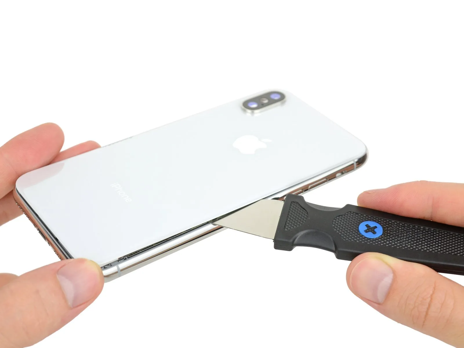
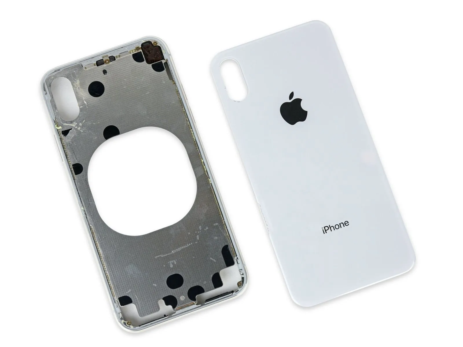
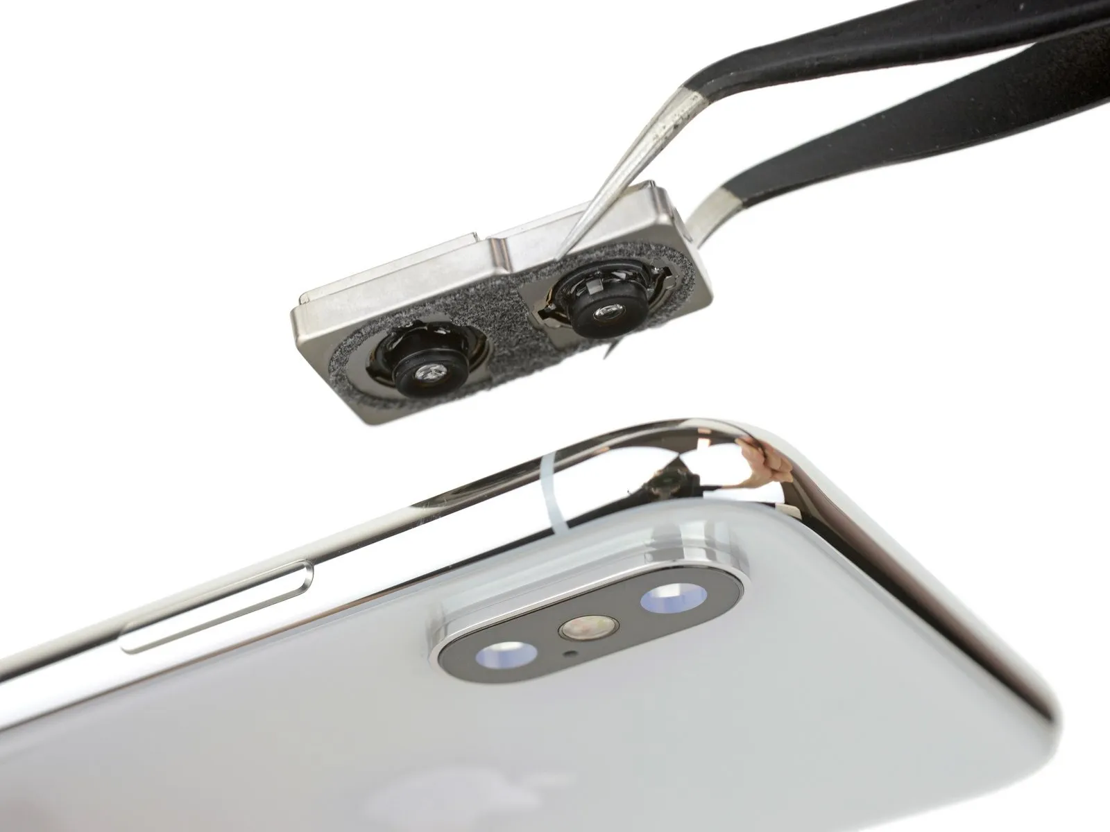
Following extensive application of heat, the spudger was retracted, and a Jimmy was employed. Mirroring the iPhone 8 and 8 Plus models, the iPhone X incorporates a rear panel that is exceptionally well-bonded.
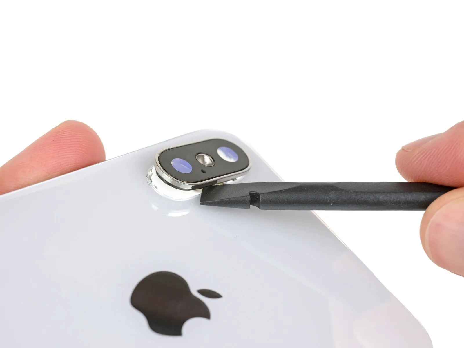
Despite our meticulous efforts using the Jimmy tool, we remain impeded; the camera module extends over the rear glass, and is precisely fused to the underlying metal frame, differing from the iPhone 8's single-piece rear panel.
This predicament, akin to having one's hand caught in a cookie jar, presents a choice: either sacrifice the camera module or fracture the rear glass. The situation is less than ideal.
We choose to remove the camera module to preserve the glass panel. Individuals replacing a damaged panel will find themselves without viable alternatives, and will encounter significant difficulty in removing the fragments of glass adhered by adhesive.
Step 24
Should you have overlooked the teardown guides for the iPhone 8 or iPhone 8 Plus, we encourage you to review them for comparative analysis. Furthermore, you are welcome to consult our Smartphone Repairability assessment to view prior device performance ratings.
Our sincere gratitude goes to our invaluable collaborators, Circuitwise, Creative Electron, and TechInsights!
If you desire a view of your phone’s internal components without physical disassembly, please explore our high-definition transparent and X-ray iPhone X wallpapers.