iPhone X Wireless Charging IC Replacement
Prior to commencing any repair work, confirm the device is completely disconnected from all electrical power.
- Necessary Tools:A Phillips head screwdriver is needed.
Consult the device's user manual to obtain precise specifications for your particular model and to review supplementary safety guidelines.
Step 1 | iPhone X Wireless Charging IC Replacement
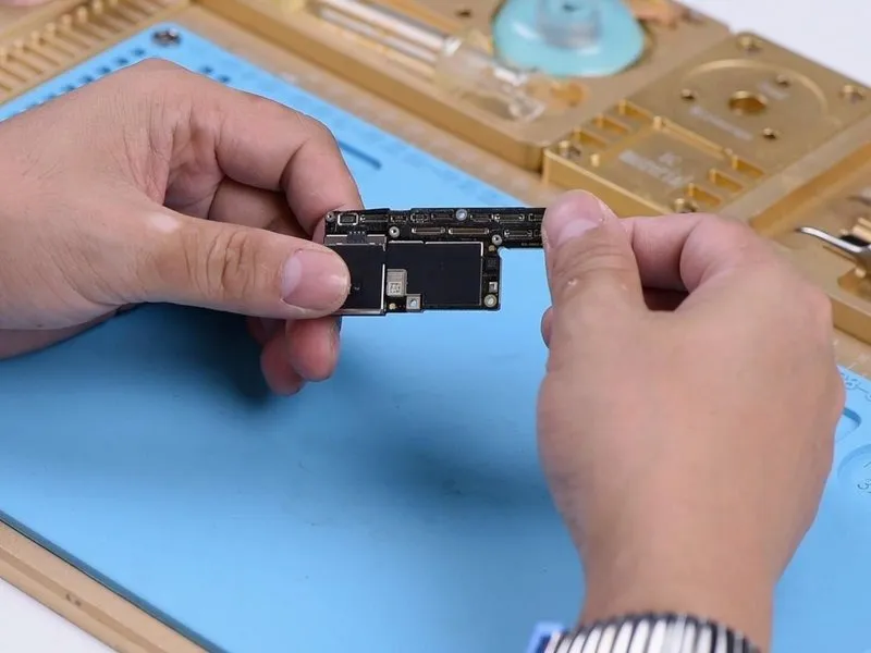
- Initially, perform a visual assessment of the motherboard.Conduct a superficial examination.Verify the motherboard's physical condition, ensuring it exhibits no warping or signs of water exposure.
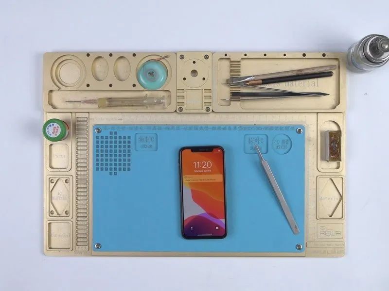
- Subsequently, reassemble the device and proceed with functional testing.
Activate the device by depressing the power button; it should power on without issue.
Step 2
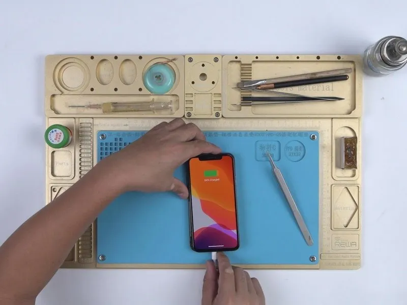

- Connect the specified cable to initiate power transfer.Utilize the provided charging cable for electrical replenishment.Electrical power can be delivered to the device through the charging cable.
- Position the device atop a compatible wireless charging base; however, wireless charging functionality is currently unavailable.
Our attention should be directed towards the electronic components responsible for wireless charging capabilities.
Step 3

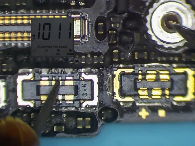
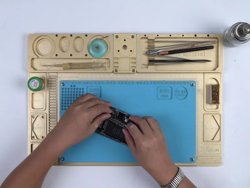
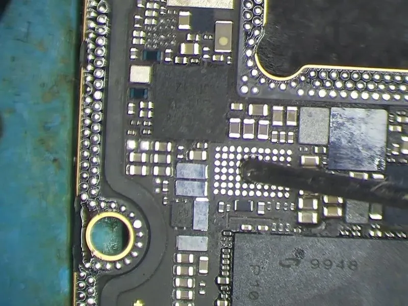
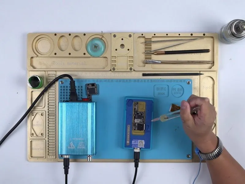
- Disassemble the device and extract the primary circuit board, ensuring to initially remove thedust-proof spongethat shields the board's surface.
Subsequently, perform a diode mode test on the wireless charging connector; a standard reading confirms the integrity of the wireless charging circuitry associated with the bonding pad, necessitating a shift in focus to the corresponding circuits located on the underside of the board.
Step 4
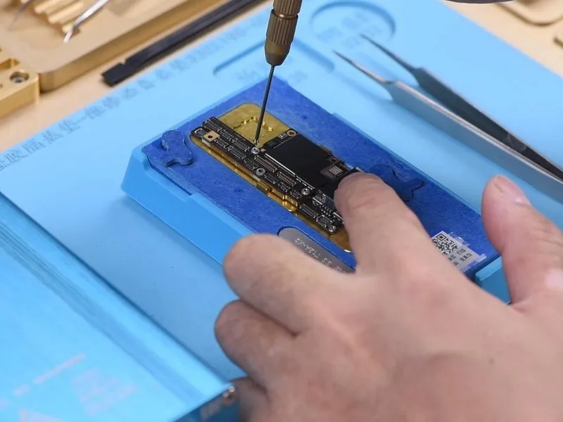


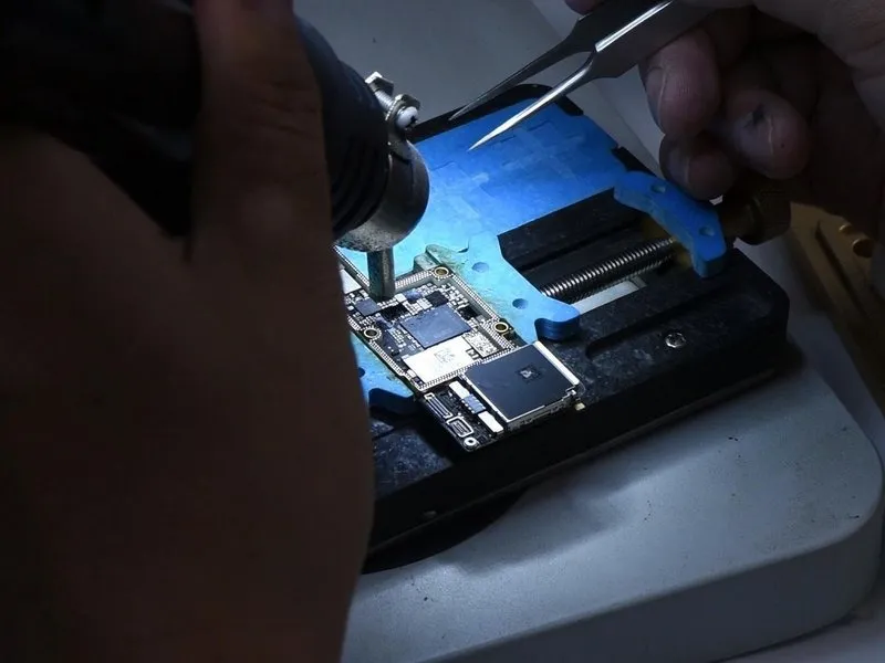
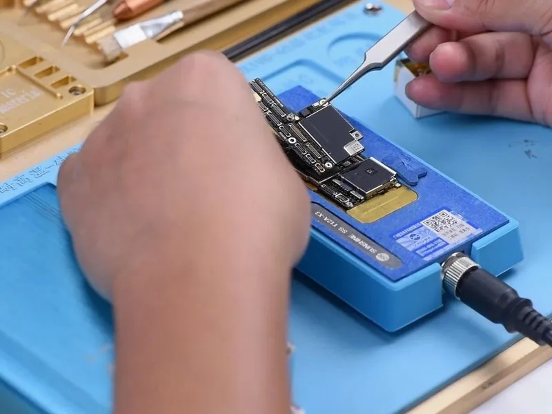
- Initially, detach the upper assembly from the underlying base.
Secure the motherboard onto the heating surface using a screw inserted into the designated screw aperture, facilitating subsequent removal of the upper layer.
Apply heat to the motherboard for a duration of 2 minutes on the heating platform at a temperature of165°C.
Following the heating process, carefully remove the upper layer utilizing tweezers, and then proceed to remove the lower layer.
Step 5
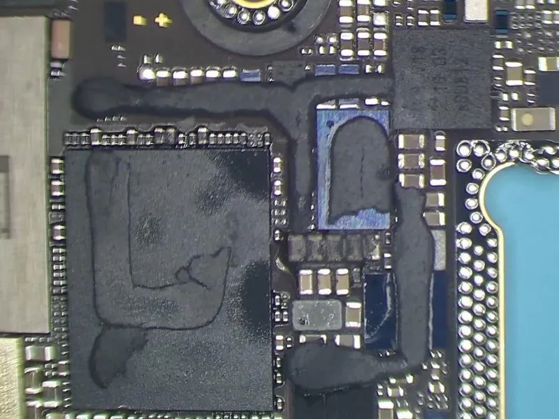

- Carefully examine the lower layer for any visible defects or anomalies, noting that no issues are anticipated.
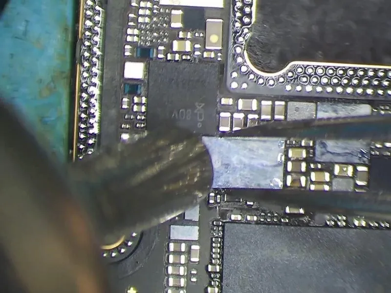
- Employ a diode mode measurement technique on the capacitors situated near the wireless charging integrated circuit; the resulting readings indicate the absence of any short circuits.
- Proceed with diode measurements around the wireless charging IC, confirming that the values obtained remain within the expected normal range.
Step 6

Proceeding to step 6:To troubleshoot further, attempt substituting the wireless charging IC with a fresh component and evaluate the results.
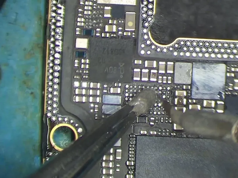
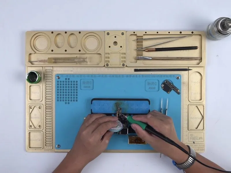
- Secure the bottom section of the printed circuit board within the PCB holder, then apply a thin layer of paste flux onto the wireless charging IC's location.
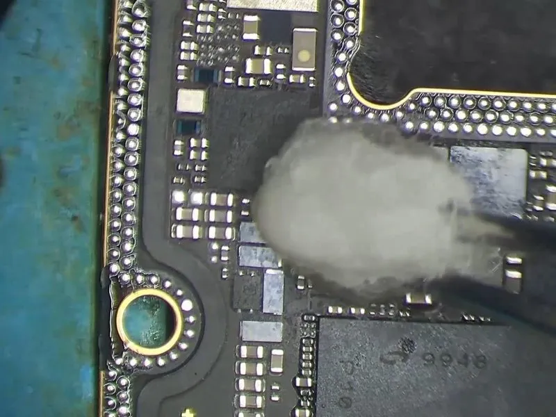
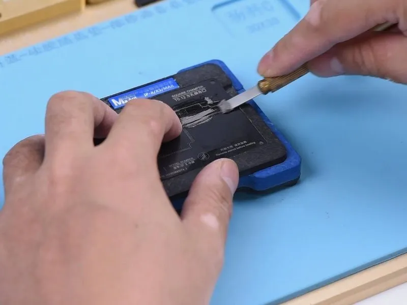
- Utilizea QUICK 990 AD Hot Air Gunset to 360 degrees Celsius, with an airflow setting of 3, for approximately 60 seconds. Carefully detach the wireless charging IC from the circuit board using tweezers.
- Subsequently, apply a moderate amount of medium-temperature solder paste to the bonding pad area and employ a soldering iron set to 365 degrees Celsius to thoroughly clean the pad.
Step 7
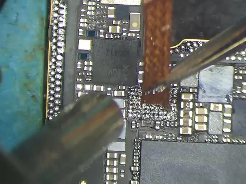
Procedure 7:After completion of the previous action, utilize a Hot Air Gun, set to a temperature of 360°C and an airflow rate of 3, to remove residual flux using rosin-impregnated solder wick from the bonding pad’s surface.
- Subsequently, employ a PCB cleaning solution to ensure complete residue removal, and then apply a thin layer of flux paste to the bonding pad.
Step 8

Proceed to step 8:Secure a replacement wireless charging integrated circuit, ensuring correct placement, and then apply heat using a soldering iron.Utilize a QUICK 990 AD Hot Air Gun for the soldering process.Set the device to a temperature of 360 degrees Celsius and maintain an airflow rate of 3.
Step 9
Phase Nine:To proceed, the two circuit board layers must now be joined via soldering.
- Prior to applying heat, ensure the bonding pad is free of contaminants.
- Following the soldering process, the bonding pad requires reballing.
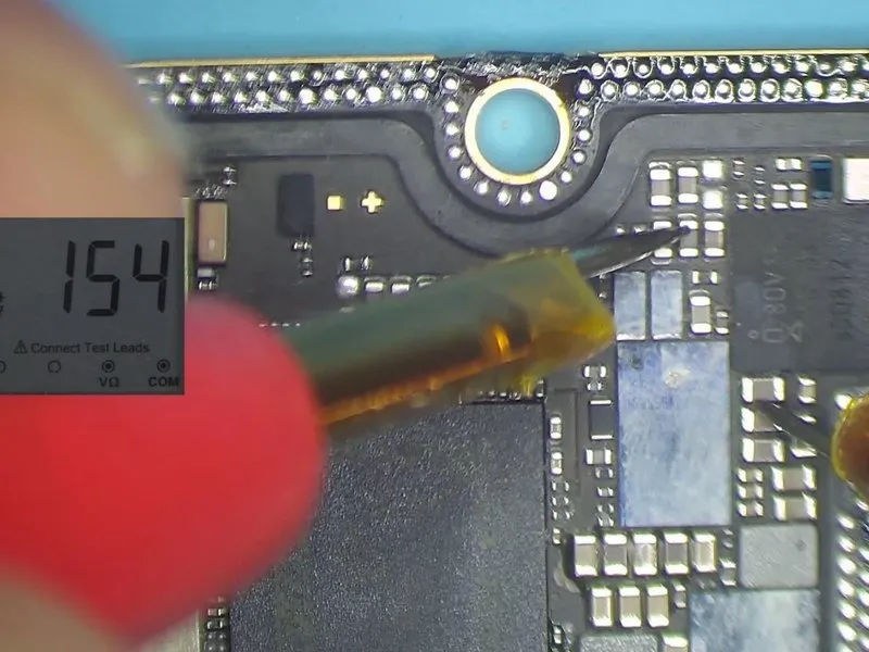
Step 10
Phase 10:After the previous actions are finished, position the bottommost component on the heated surface. Utilize BGA paste flux on the contact area and carefully align the uppermost component.
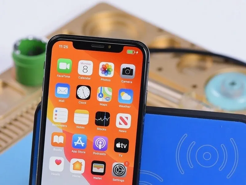
To verify wireless charging capability, position the device on a compatible wireless charging base.
- Maintain a temperature of 165°C on the heating platform for a duration of 2 minutes.
To verify wireless charging capability, position the device on a compatible wireless charging base.