Repair iPhone X Battery that Drains Fast
Prior to commencing any repair work, it is essential to disconnect the device entirely from all electrical power supplies.
- Necessary Tools:A Phillips head screwdriver is needed for this procedure.
Consult the device's user documentation to obtain precise specifications for your particular model and to review supplementary safety guidelines.
Step 1 | Battery
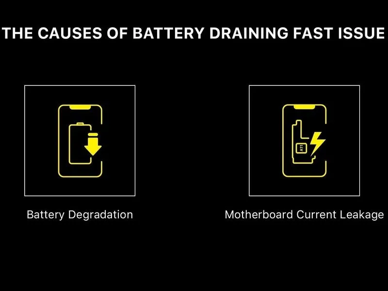
- A rapidly depleting battery accompanied by excessive heat is observed in the iPhone X.
- Accelerated battery discharge is frequently attributable tothe natural decline in battery capacity over timeoran unintended flow of electrical current from the device's main circuit board.
- Even following a battery substitution, continued rapid battery depletion suggests the root cause lies withinan unintended flow of electrical current from the device's main circuit board.
Step 2
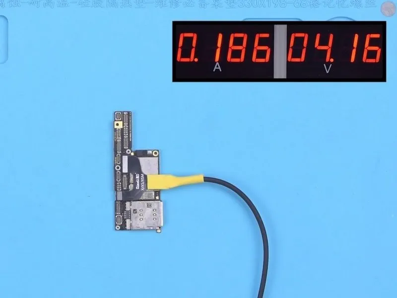
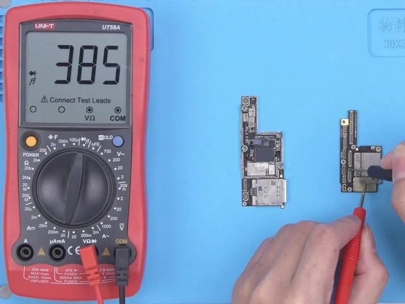
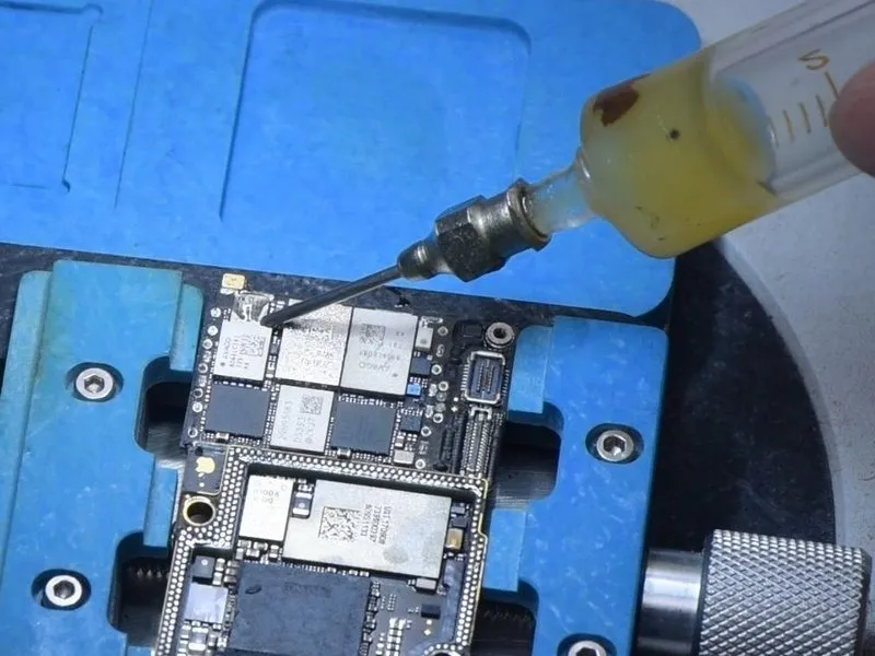
Following this, assess the electrical flow by activating the motherboard using a direct current power source, as the motherboard exhibitsa current leakage measuring 186 milliamperes.
Step 3


Should a motherboard exhibit a condition of current leakage upon activation, it becomes possible to evaluate the subsequent power supply pathways to pinpoint the defective component.
Step 4


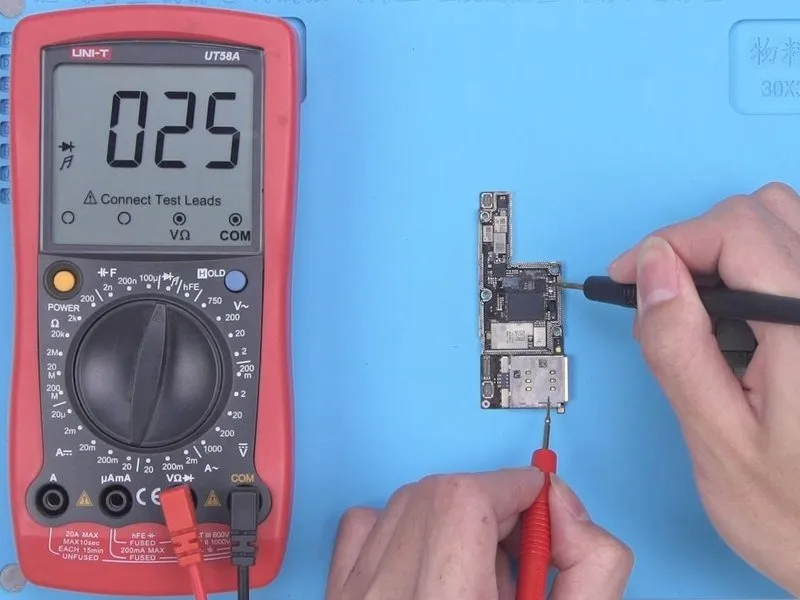
- Initially, assess PP_BATT_VCC. The observed resistance aligns with expected norms.
- Subsequently, evaluate PP_VDD_Main. A resistance of 29 ohms is detected, which is notably low, suggesting a compromised component on PP_VDD_Main. Due to the limited current flow, standard rosin detection methods are ineffective in pinpointing the precise location of the fault; consequently, a thermal imaging device is required for identification.
Step 5
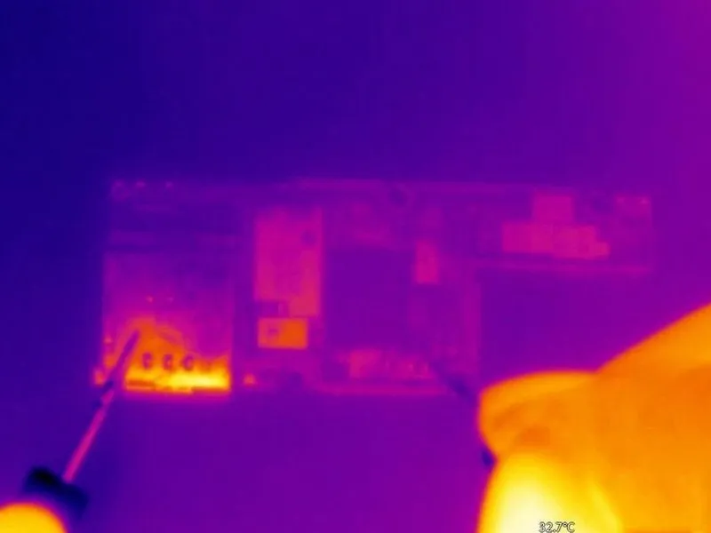

- Activate electrical power to the PP_VDD_Main located on the motherboard; observe that no visible temperature fluctuations are present, indicating the defective component is not readily accessible on the exterior of the circuit board.
- Subsequently, disconnect the motherboard to facilitate more detailed diagnostics. Position the motherboard upon a Heating Platform and elevate its temperature. Once the temperature achieves 165 °C, detach the logic board from the signal board.
Step 6
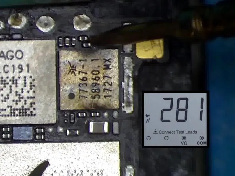
- Once the motherboard has reached ambient temperature, utilize a multimeter to assess the resistance at the designated test point, PP_VDD_Main which should register within expected parameters.
- Subsequently, perform a similar resistance measurement at PP_VDD_Main located on the signal board; a deviation from the normal range indicates a defect within the signal board's components.
Step 7
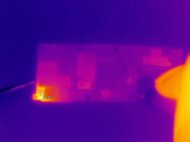
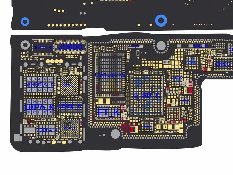
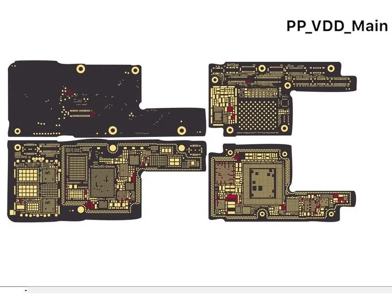
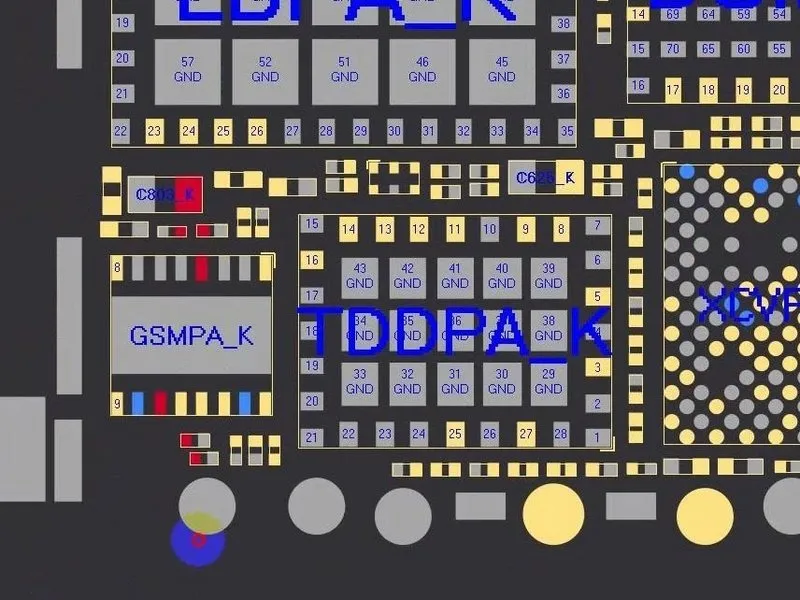
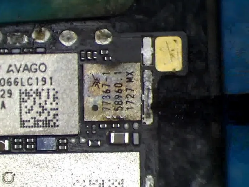
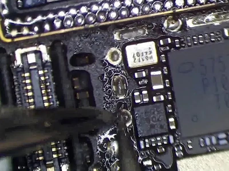
- Verify the location of using the provided bitmap image.PP_VDD_MainContinue monitoring the signal board's temperature distribution using a thermal imaging device; no significant temperature variations are currently detectable.
- Examination of the bitmap reveals thatPP_VDD_Mainis also situated beneath the card reader.
Step 8

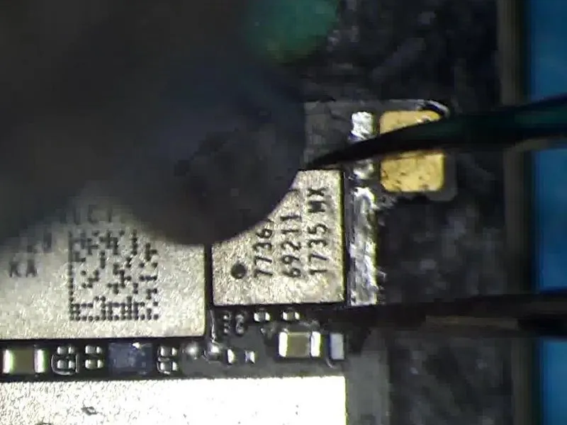
- The defective component is probably located beneath the card reader assembly; utilize a Thermal Imager to examine the rear surface of the signal board. A significant temperature increase has been observed in the upper-left corner of the card reader.
- Verification indicates the problematic component resides within the card reader region.
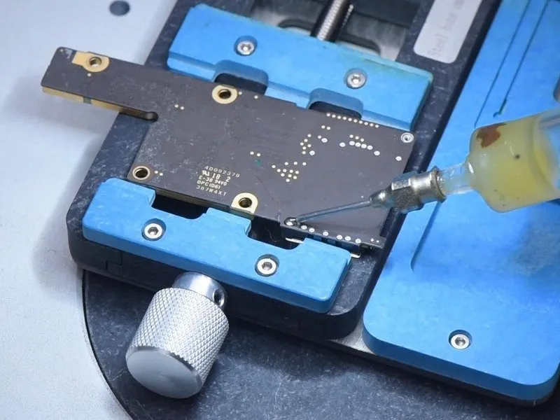
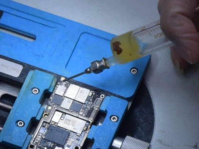
- Proceed with card reader removal. Apply Paste Flux to the card reader's bonding pad. To safeguard the plastic components, apply low-temperature Solder Paste to mitigate the bonding pad's heat.
Step 9

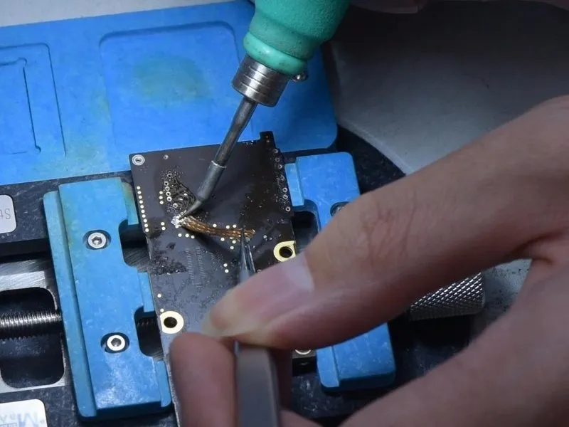
- Subsequently, employ ahelical wind Hot Air Gunat a temperature of340 degrees Celsiusto apply heat to the card reader assembly. Simultaneously, utilize aPry Bladeto gently lift the card reader during the heating process.
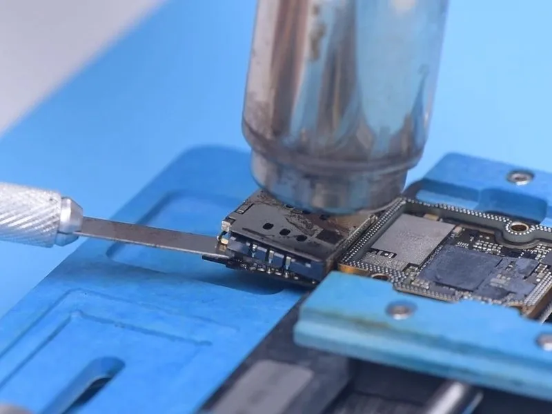
- Once the card reader disengages, carefully detach it from the board.
- Continuously monitor the card reader region with a Thermal Imager; substantial temperature variations will be apparent in this area.
- Based on the visual representation, the component exhibiting elevated temperatures is theGSMmodule.Then, substitute the defectiveGSM
Step 10

- To facilitate soldering, apply Paste Flux. Subsequently, remove theGlobal System Moduleutilizing a downward airflow from aHot Air Gunmaintained at a temperature of340 degrees Celsius.
- Following component removal, apply Paste Flux and middle-temperature Solder Paste to the bonding pad; this process reduces the thermal stress experienced by the bonding pad during subsequent operations.
Step 11
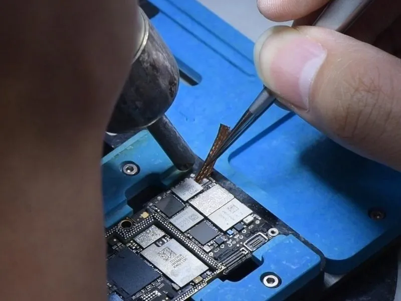
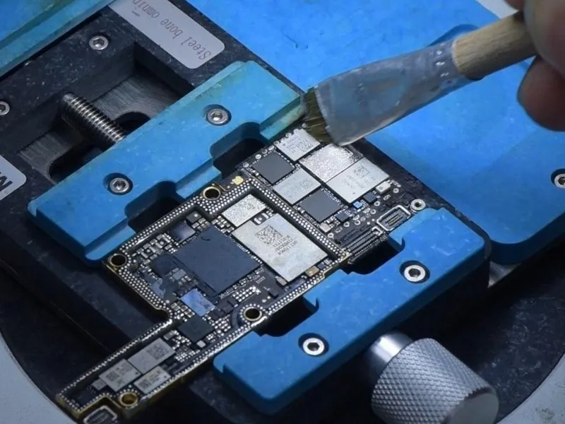

- Utilize a cleaning agent and prepare the bonding pad for subsequent steps.Employ a Hot Air Gun to facilitate the removal of excess material.Additionally, incorporate Solder Wick into the cleaning process.Following the initial cleaning, apply PCB Cleaner to ensure a pristine surface.Subsequently, determine the electrical resistance of PP_VDD_Main.PP_VDD_Main is the component whose resistance will be assessed..
- Successful completion of the procedure will result in a return to expected resistance levels.
Step 12
- Subsequently, mount a verified functional GSM. Utilize Paste Flux for enhanced adhesion. Position the GSM securely. Employ a vertical airflow technique with a Hot Air Gun set to a temperature of 320 °C.
- Following the soldering process, re-verify the electrical connection using a multimeter; a standard resistance reading confirms proper functionality.
Step 13

- Continue to apply a thin layer of Solder Paste to the designated bonding area on the card reader's surface.
- Employ a cleaning process utilizing aHot Air Gunalong withSolder Wickto remove excess material. Subsequently, utilize aSoldering IronandSolder Wickto cleanse the rear bonding pad.
Step 14

- Subsequently, utilize PCB Cleaner to remove contaminants, confirming the pins are free from residue.
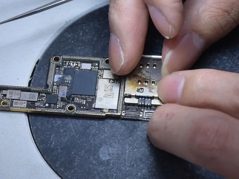
- Following this, mount the card reader, ensuring precise alignment within its designated location.
- Secure the card reader to the board by soldering the rear bonding pad, employing aSoldering Ironto achieve a robust connection.Remove surplus solder withSolder Wick
- Finally, employ PCB Cleaner to eliminate any remaining flux or residue from the bonding pad.
Step 15


- Reassemble the main circuit board, positioning the signal board onto a heated surface.Utilize a 165 °C Heating Platform to provide thermal energy.Introduce Paste Flux onto the bonding area, carefully align the logic board with the signal board, and release the motherboard once the temperature stabilizes at 165 °C.
- To ensure a secure reconnection, apply slight pressure to both edges of the motherboard using tweezers.
- Initiate power to the motherboard and perform a functional assessment, confirming the electrical current is within expected parameters.
Step 16

- To verify functionality, establish a connection between the display panel and the system.
- Measurements confirm the boot sequence is drawing the expected electrical current.
- The issue of excessive current leakage has been successfully resolved.